



Content last revised on September 27, 2026
TT250N18KOF12M1 Thermal-Electrical Optimization: RC Damping in Practical Tuning
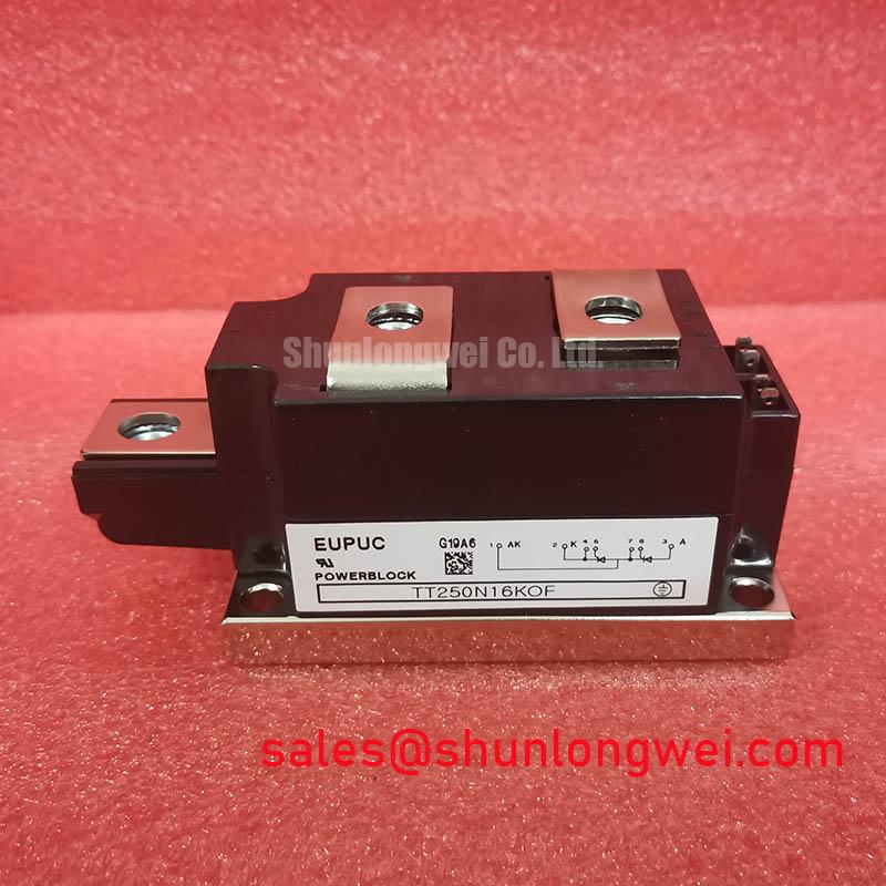
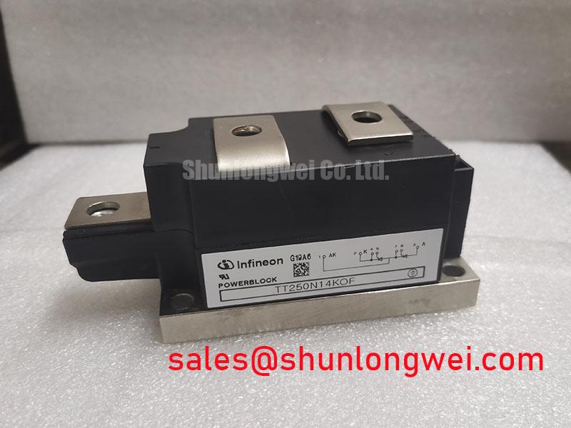
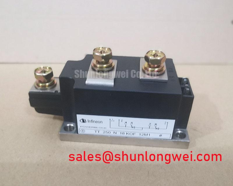
Begin commissioning by checking the nameplate against the required 1800 V rated voltage and 250 A rated current, then inspect the PowerBlock housing, terminals, and mounting surface for damage or contamination before applying power. These are product specifications for the Infineon TT250N18KOF12M1; gate, surge, thermal-resistance, fuse coordination, and mechanical torque values should be verified against the applicable manufacturer datasheet before system release.
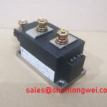
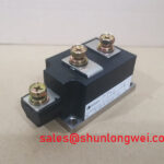
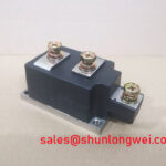
The device is identified as a Dual Thyristor Module in a PowerBlock Module package. Its electrical ratings make it a candidate for evaluation in controlled industrial power-conversion equipment, including medium-frequency induction melting and metal hardening power supplies. Final suitability depends on the circuit topology, firing control, cooling system, fault protection, and the repetitive current waveform.
In an induction heating power supply, the commutation network and transformer leakage characteristics determine the voltage and current stress seen by each thyristor. An RC snubber should therefore be evaluated as part of the complete switching loop rather than selected from the module current rating alone. The design objective is to control transient voltage rise and prevent unintended triggering caused by coupling through the gate and power circuits.
Designers should verify the required resistor and capacitor ratings from measured switching waveforms, the expected repetition rate, and the actual energy handled by the snubber. A series saturable reactor may also be assessed where the system requires controlled current rise during turn-on. Its selection remains system-determined and should be confirmed through thermal testing and oscilloscope measurements at the module terminals.
Fuse coordination must use the applicable manufacturer data, including the relevant I²t relationship and prospective fault current. The supplied product information confirms the voltage, current, and package category, but does not provide a fuse I²t table here. Do not infer a protection value from the 250 A rating alone.
Assembly Integrity & Layout Architecture: Coordinating Surge Protection and MOVs for TT250N18KOF12M1
High-energy AC input protection should be coordinated in stages. A primary surge diversion path, suitable MOV network, and local RC suppression can be evaluated according to the equipment insulation system and the surge environment. IEC 61000-4-5 test planning may be relevant to the finished equipment, but the thyristor module itself should not be described as independently EMC-certified.
Keep the high-current path physically compact and symmetrical where the circuit uses paired thyristor paths. Minimize stray inductance in the commutation and snubber loops, while keeping control wiring separated from rapidly changing power conductors. The gate driver should be checked for adequate noise immunity, controlled turn-on timing, and protection against false firing. For isolated industrial drive boards, the selected optocoupler or digital isolator should be evaluated for common-mode transient performance suitable for the measured switching environment.
Terminal identification, conductor cross-section, creepage, clearance, and enclosure insulation must be checked against the original equipment documentation and applicable system standards. Bench Diagnostic: isolate and discharge the power stage before removing any gate or power connection. Mounting torque must follow the applicable Infineon mechanical specification; no torque value is asserted here because it was not included in the supplied factory parameter set.
For a neutral comparison during sourcing, engineers may review the electrical role and package requirements of the TT570N16, but any substitution requires a complete verification of voltage, current, triggering, thermal, mechanical, and protection compatibility.
Field Diagnostics & Commissioning: Thermal and Surge Margins in TT250N18KOF12M1 Topologies
Commissioning should begin with low-energy gate checks and continuity observations performed with the power stage isolated. The engineer can then compare the firing sequence, anode-cathode voltage, load current, and commutation interval against the known-good circuit path. An abnormal waveform may indicate a gate timing issue, commutation interaction, insufficient suppression, or an installation problem; confirm the cause with measured evidence rather than assigning it to the module immediately.
The sinusoidal half-cycle surge rating, commonly identified in thyristor documentation by ITSM, was not included in the supplied parameter list and must be taken directly from the applicable datasheet. The same applies to gate trigger current, gate trigger voltage, holding current, latching current, junction temperature, and thermal resistance. Before forward blocking voltage is reapplied, verify that the circuit has completed commutation and that measured voltage and temperature remain within the manufacturer’s limits.
For battery-supported bidirectional DC-DC systems using a thyristor-based topology, repeated charge and discharge cycling can create thermal transients at the module and heatsink interface. Designers should record case temperature, switching interval, load current, and cooling conditions across the intended operating profile. Lifetime or failure-rate claims require qualified field or laboratory sources and should not be inferred from the nominal current rating.
Infineon’s information on automotive-qualified power modules and intelligent power modules provides useful context for distinguishing module families; it does not replace the specific thyristor datasheet for this product.
Benchtop Waveform Tuning: Mitigating Stress Through Thermal Interface Material Application on TT250N18KOF12M1
Thermal evaluation should start by confirming that the heatsink contact surface is clean, flat, and free from burrs. Apply the thermal interface material according to the material supplier’s process instructions, then tighten the module using the manufacturer’s specified sequence and torque. Uniform contact pressure is important because local mounting distortion can increase thermal impedance or place mechanical stress on the PowerBlock package.
Measure case temperature at a repeatable location while recording load current, ambient conditions, firing angle, and cooling airflow or coolant conditions. The applicable datasheet value for junction-to-case thermal resistance, Rth(j-c), must be used when converting measured case temperature into a junction-temperature estimate. That value was not provided in the supplied factory parameter table, so a numerical thermal limit should not be assumed.
During waveform tuning, inspect turn-on and turn-off behavior at the module terminals, including any overshoot, ringing, unequal current sharing, or delayed commutation. Minimize parasitic loop inductance to reduce transient stress, then verify peak margins against the system voltage and current limits during controlled switching tests. The technical background of wide-bandgap power conversion can be reviewed in this Wide Bandgap Revolution resource, while the integration decision for this silicon thyristor module remains dependent on the measured application conditions.