

Content last revised on October 8, 2026
Static and Dynamic Current Distribution across Paralleled IGBT Switches
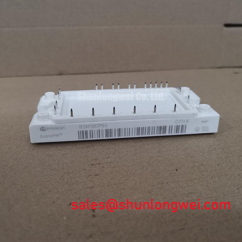
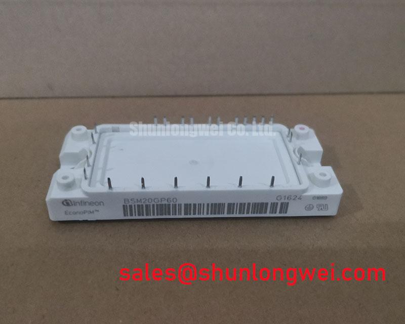
Before fitting the device into a servo inverter, verify the nameplate against the original service documentation and perform a controlled cold-state inspection of the power terminals, mounting surface, and gate-drive connection. The Infineon BSM20GP60 is specified as a 600 V, 20 A IGBT module in a Module package. These are product parameters supplied for this product record; switching frequency, gate-charge data, thermal resistance, internal circuit topology, isolation rating, and terminal arrangement should be confirmed from the applicable manufacturer documentation before circuit replacement.
High-dynamics multi-axis CNC and robotics servo drives can place several switching devices in parallel when the converter requires greater current capability. In that arrangement, static sharing is influenced by the positive temperature coefficient commonly associated with IGBT collector-emitter saturation voltage in the relevant operating region. A warmer device may develop a higher conduction voltage, allowing part of the load current to redistribute to cooler devices. This behavior supports current balancing, but it does not remove the need for matched electrical paths and thermal conditions.
Dynamic sharing is controlled more strongly by the gate-drive network, commutation loop, and stray inductance. Each parallel branch should use a geometrically similar power path, with matched collector and emitter connection lengths and comparable contact resistance. Keep the high-current commutation loop compact and avoid routing a gate signal beside a rapidly changing collector node. If the original module documentation identifies a separate auxiliary emitter or Kelvin emitter connection, its return should be routed directly to the driver reference rather than sharing a long high-current emitter path. Do not assume that every module terminal arrangement includes such an auxiliary connection.
During field troubleshooting, compare the gate-emitter waveform of each branch with an oscilloscope using an appropriate differential or isolated measurement method. Look for unequal turn-on delay, different Miller plateau behavior, overshoot, or ringing between branches. These observations may indicate unequal gate resistance, connector resistance, driver timing, or layout inductance. A cold resistance check can identify an open interconnect, but it cannot validate dynamic current sharing under switching conditions.
💡 Pro Tip: Treat the gate loop as a high-frequency power circuit: minimize its area, keep the driver return paired with the gate path, and validate the resulting waveform at the module terminals rather than only at the driver output.
For a neutral comparison during service planning, engineers may review the electrical and mechanical documentation for FF150R12ME3G. It should not be treated as a drop-in replacement without checking voltage class, current rating, internal topology, terminal geometry, gate-drive requirements, thermal interface, and control-system limits.
Regenerative DC-Bus Voltage Surge Dissipation during Rapid Machine Deceleration
Rapid deceleration returns motor energy to the DC bus. The braking path must therefore be evaluated as a complete energy-handling circuit rather than by selecting an IGBT from its current rating alone. Confirm the servo drive’s DC-bus operating range, braking duty profile, resistor pulse capability, switching interval, and protective threshold. The BSM20GP60 product record specifies a 600 V voltage rating and a 20 A current rating; these values do not by themselves establish a permissible braking-energy profile or safe operating area for a particular machine.
The braking IGBT and ballast resistor should be assessed against the highest expected regenerative event, including repeated stops, line-frequency bus ripple, and the thermal recovery time between braking pulses. Duty control can regulate the energy transfer into the resistor, but the control loop must be coordinated with bus-voltage sensing and gate-driver delay. A practical commissioning procedure is to begin with a controlled low-energy stop, record the DC-bus waveform, and then increase the deceleration demand only after peak voltage, current, and device temperature remain within the system design limits.
Busbar geometry is critical during turn-off. Stray inductance can convert rapid current change into collector-emitter overshoot, so the DC-link capacitor, braking switch, and high-power resistor connection should be arranged to reduce the commutation loop area. RC snubber selection is system dependent. The capacitor must tolerate the transient current and voltage, while the resistor must dissipate the associated pulse energy without becoming an additional failure source. Verify the snubber with an oscilloscope at the power terminals, not solely through a controller diagnostic value.
A front-end or auxiliary topology may include a separate high-power device such as BSM100GAL100D. Its presence in a system does not define compatibility with the BSM20GP60; confirm the actual schematic, isolation arrangement, and control sequence before connecting complementary stages.
Junction-to-Case Thermal Network Simulation under High-Pulsed Overloads
Short overloads in servo applications can be electrically acceptable while still producing excessive junction temperature if the thermal path is poorly modeled. A thermal review should begin with the real pulse profile: current amplitude, pulse duration, repetition rate, duty cycle, and cooling condition. Use the manufacturer’s verified transient thermal data where available. If those curves are not available for the exact device configuration, a multi-resistor and capacitor thermal model can be used only as an engineering approximation and must be validated by measurement.
The calculation should combine conduction loss and switching loss over the actual waveform, then propagate the resulting power pulses through the junction-to-case and case-to-heatsink paths. Peak junction temperature depends on the initial case temperature and the transient thermal impedance at the pulse duration, not simply on average power. The thermal interface should be flat, clean, and evenly clamped. Confirm that the mounting hardware, insulator, and heatsink arrangement match the original mechanical design.
Field diagnosis should compare temperature rise at equivalent load points, inspect the interface for uneven contact, and check that cooling airflow or liquid flow is not obstructed. An abnormal thermal rise may originate from excessive switching loss, poor clamping, degraded interface material, an inaccurate temperature sensor, or an unbalanced parallel branch. Separate these possibilities by measuring collector-emitter behavior, gate timing, case temperature, and cooling performance under a controlled test profile.
Use the Field Engineer’s Handbook as a practical reference when organizing measurement records, failure analysis, and repeatability checks. It should supplement, not replace, the applicable Infineon device documentation and the machine manufacturer’s service limits.
Isolated DC-DC Power Supply Sizing for High-Side Floating Gate Drivers
A high-side floating gate driver requires a supply that remains stable while its reference node moves with the switching device. Size the isolated DC-DC stage from the driver’s quiescent current, gate-charge demand, switching frequency, startup behavior, protection current, and transient recovery requirement. The BSM20GP60 entry does not provide gate-charge, driver-supply, isolation, or common-mode transient immunity figures, so those values must be verified from the exact module and driver documentation rather than inferred from the voltage and current ratings.
Isolation coordination should consider the complete barrier, including the DC-DC transformer, driver IC, PCB creepage and clearance, insulation system, and test method. A design requirement such as reinforced isolation or a specific common-mode transient immunity level belongs to the assembled gate-drive system and must be verified against the applicable safety and functional requirements. It is not an automatic specification of the IGBT module.
Place the isolated supply decoupling close to the driver pins and keep the floating power loop separate from the high-current commutation path. Gate resistance, Miller-current control, and any active-clamp function should be selected from the driver and switching-waveform requirements. During validation, monitor the isolated supply, gate-emitter voltage, collector-emitter voltage, and driver reference together. Spurious gate pulses may arise from inadequate decoupling, common-mode coupling, driver saturation, or measurement error, so the diagnosis should compare the faulty channel with a known-good channel under the same switching conditions.
For authoritative background on power semiconductor families and application documentation, consult Infineon High Power Semiconductor Solutions. Final integration should be released only after the complete servo inverter has passed its electrical, thermal, isolation, and switching-transient verification defined by the equipment design authority.