



Content last revised on November 12, 2026
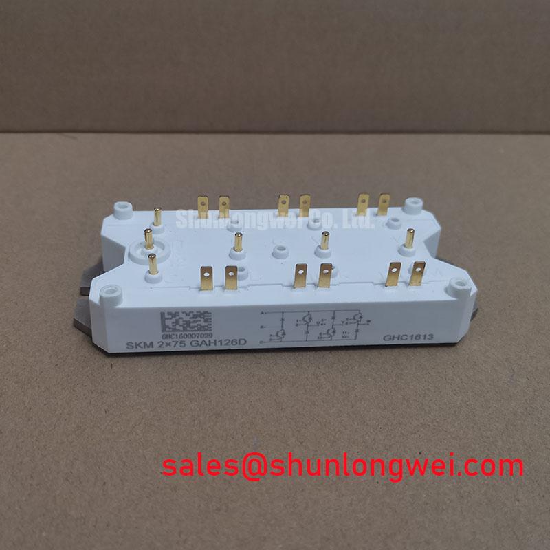
SKM2X75-GAH126D Identification and Incoming Inspection
- Isolate the DC link, verify discharge with suitable test equipment, and identify collector, emitter, and gate connections from the terminal drawing before taking resistance readings.
- Record cold-state collector-to-emitter and gate-to-emitter measurements with the module disconnected from external paths that could influence the results.
- Check the mounting surface, terminal alignment, and thermal-interface condition before comparing the replacement module with the removed assembly.
- Inspect the gate-driver isolation barrier and emitter return routing before reconnecting the power stage.
The SKM2X75-GAH126D is a Semikron IGBT Module with the electrical and housing specifications below. For incoming inspection, establish terminal identity before interpreting any meter reading: an external gate resistor, discharge network, or connected driver can change the apparent resistance without identifying a module defect.
| Specification | Product value |
|---|---|
| Manufacturer | Semikron |
| Part Number | SKM2X75-GAH126D |
| Product Category | IGBT Module |
| Collector-Emitter Voltage (Vces) | 1200.0 V |
| Continuous Collector Current (Ic) | 275.0 A |
| Package | Semitrans |
| Configuration / Topology | IGBT Power Stage |
| Additional integration details | Consult Datasheet for terminal assignments, rating conditions, gate limits, insulation test conditions, and mounting requirements. |
The electrical entries are product specifications, not bench acceptance thresholds. In particular, the collector-current rating requires its associated thermal conditions when assessing continuous operation. The engineering guidance below is identified as Design Consideration; it does not add manufacturer-guaranteed characteristics to this model.
💡 Bench Tip: Use ESD protection and a consistent discharged-gate condition when comparing cold-state readings with a known-good reference.
Preventing Spurious Faults: Suppressing C_res-Induced Gate Voltage Spikes in SKM2X75-GAH126D Applications
Measure the gate-to-emitter waveform at the module connection during complementary-switch transitions, rather than relying solely on the driver output pin. As a Design Consideration, collector voltage transitions couple displacement current through the reverse-transfer capacitance, commonly described as C_res. Impedance in the gate turn-off path can convert that current into an unwanted gate-voltage excursion. A pulse observed at the driver connector can differ materially from the voltage actually reaching the device terminals.
Use a suitable differential measurement arrangement with short connections and adequate common-mode capability. Compare the off-state gate waveform with collector voltage, switching current, and the complementary gate command. A brief disturbance does not by itself establish cross-conduction: probe pickup, emitter-reference movement, and driver supply disturbance can produce similar traces. Correlation across these signals is more useful than interpreting one waveform in isolation.
A dedicated active Miller clamp can provide a low-impedance discharge path while the switch is commanded off. Its effectiveness depends on clamp engagement timing, placement, and the connection back to the relevant emitter reference. Negative gate bias is another system-level option, but its magnitude must remain within the module and driver limits. Neither a clamp nor negative bias compensates for an unnecessarily long gate loop or a shared return carrying substantial power-current transients.
Inspect the physical gate loop for separated outgoing and return conductors, unnecessary connector length, and routing alongside switching-node copper. Keep the gate return closely associated with its gate conductor and control coupling from the power loop. Gate damping should be selected through controlled switching measurements: excessive resistance can increase switching loss, while insufficient damping can leave oscillation unresolved. The appropriate balance depends on the installed driver, interconnects, and operating conditions.
For cold-state screening, disconnect the driver and compare gate-to-emitter resistance in both meter polarities under consistent conditions. Where the verified circuit diagram identifies an antiparallel diode path, diode-mode measurements can compare its directional behavior with an equivalent known-good path. Record meter type, polarity, and module temperature. A handheld meter reading is not a substitute for blocking-voltage testing, and no universal forward-drop threshold establishes acceptance for this part.
Protection behavior also belongs in the gate-drive assessment. As a Design Consideration, desaturation monitoring evaluates abnormal collector-emitter voltage while conduction is commanded; its blanking and response must distinguish switching transients from a genuine fault. A controlled soft turn-off can reduce interruption-induced overshoot, but the complete detection and shutdown interval must fit the applicable short-circuit safe operating conditions. Do not infer a short-circuit withstand time from the stated current rating.
If the assembly uses parallel power paths, compare gate timing and current distribution across those paths rather than assuming equal sharing. A positive on-state temperature coefficient can assist static sharing only in the operating region where the device characteristics support it; that characteristic is not established here for this model. Dynamic sharing also depends on gate-loop symmetry, interconnect impedance, and thermal contact.
SKM2X75-GAH126D Operational Boundaries: Evaluating Output Sinusoidal Filter vs dv/dt Reactor Limits
Separate the voltage measured at the module switching node from the voltage measured at the motor terminals before selecting an output filter. As a Design Consideration, cable propagation and impedance discontinuities can produce reflected-wave peaks at the load. Their magnitude depends on cable characteristics, transition speed, motor impedance, and pulse interaction; a remote terminal peak should not be treated as a fixed multiple of DC-link voltage.
A dv/dt reactor or filter primarily moderates voltage transition behavior, whereas a sinusoidal output filter more substantially attenuates switching-frequency content. The choice affects voltage drop, reactive current, losses, and control behavior. Compare the equipment manufacturer's permitted cable arrangement and modulation conditions with the filter's operating envelope. Select the filter from those system requirements, then verify the installed waveforms rather than treating either filter type as an automatic upgrade.
At the SKM2X75-GAH126D, assess turn-off collector-emitter peaks against the 1200.0 V blocking specification while accounting for the complete switching waveform and operating conditions. Output filtering does not eliminate overshoot generated inside the local commutation loop. Reduce unnecessary power-loop area and assess DC-link connection placement before attributing every voltage excursion to the motor cable.
RC snubbers address a different part of this problem: they can damp a characterized oscillatory network, but their resistance, capacitance, and dissipation must follow measured circuit behavior. Record ringing frequency and amplitude using a consistent probe arrangement before and after a change. A quieter voltage trace alone is insufficient evidence of improvement if the modification introduces excessive component heating or switching loss.
Upstream supply behavior should be examined separately from output filtering. In a phase-controlled input stage, firing angle influences the rectified waveform, while the DC-link network manages ripple and energy exchange. A component such as SKKL 92/12E belongs in an assessment of the relevant rectifier or thyristor-stage topology; it is not an output-filter substitute or an IGBT gate-driver component. Check its circuit role against the actual power schematic.
Commutation measurements should also consider diode reverse recovery wherever the verified circuit includes a freewheeling path. Recovery current can affect switching loss, ringing, and conducted or radiated disturbance. Recovery softness is a device characteristic requiring applicable test conditions, not a value that can be inferred from a diode-mode measurement. Compare current and voltage traces together before attributing a disturbance specifically to recovery behavior.
The VFD pump constant-pressure control guide provides related application context for investigating drive behavior, but equipment acceptance limits should come from the applicable service and design documentation. For battery charge-discharge stages, when the topology is applicable, load transitions and cooling response deserve attention because they shape junction-temperature cycling. Reducing unnecessary thermal excursions is a design objective, not grounds for assigning this module an unsupported service-life figure.
Assembly Integrity & Layout Architecture: Implementing Galvanic Gate Drive Isolation, Reinforced for SKM2X75-GAH126D
Examine the driver isolation barrier independently of the module's collector-emitter blocking rating. As a Design Consideration, galvanic isolation performance depends on the driver, isolated supply, PCB layout, connectors, and installation environment. Reinforced insulation is a classification established by the applicable safety requirements and supporting component documentation; it cannot be inferred from a package name or a high-voltage switching rating.
Check working voltage, transient exposure, pollution conditions, and required insulation category before evaluating clearance and creepage. Inspect the finished assembly for conductive contamination, misplaced fasteners, and wiring that bridges the intended barrier. Any dielectric test needs a defined procedure, appropriate equipment, and test connections that protect connected electronics. Applying an arbitrary high-voltage test to an assembled driver can be inappropriate even when the isolated components have documented test ratings.
Common-mode transient immunity concerns the driver's ability to maintain correct behavior during rapid potential changes across its isolation barrier. Compare the driver's documented test conditions with measured switching behavior, including polarity and reference arrangement. If an unexpected gate pulse appears, inspect isolated-supply stability and command-signal integrity alongside the gate waveform. A component-level immunity specification does not establish immunity for the complete installed assembly.
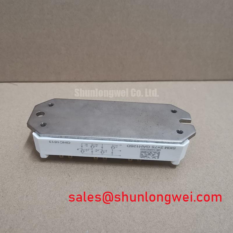
Mechanical fit requires an equally explicit comparison. The Semitrans designation identifies the stated housing family, not a complete interchangeability specification. Compare terminal position, fixing points, baseplate contact, and available insulation distances with the equipment drawing. The manufacturer's Semikron-Danfoss SEMITRANS industry-standard IGBT information provides family context; mounting instructions for the exact device govern assembly details.
For replacement evaluation, SKM400GM12T4 can be included in a documented comparison, but it should not be treated as a verified direct replacement without matching topology, terminal mapping, drive requirements, thermal performance, and mechanical fit. For electric material-handling equipment or forklift low-voltage traction repairs, first establish the installed power-stage identity; this module's stated ratings alone do not establish suitability for that application.
Before powered testing, document terminal mapping, cold-state readings, mounting condition, and driver connections on the inspection record. Where a measurement differs from the reference assembly, repeat it with external paths isolated and the same instrument setup. Resolve the discrepancy through circuit tracing and controlled testing before releasing the assembled power stage.