Content last revised on September 26, 2026
Field Diagnostics & Commissioning: Suppression of 2× VDC Voltage Doubling in SKIIP 83ANB15T4 Topologies
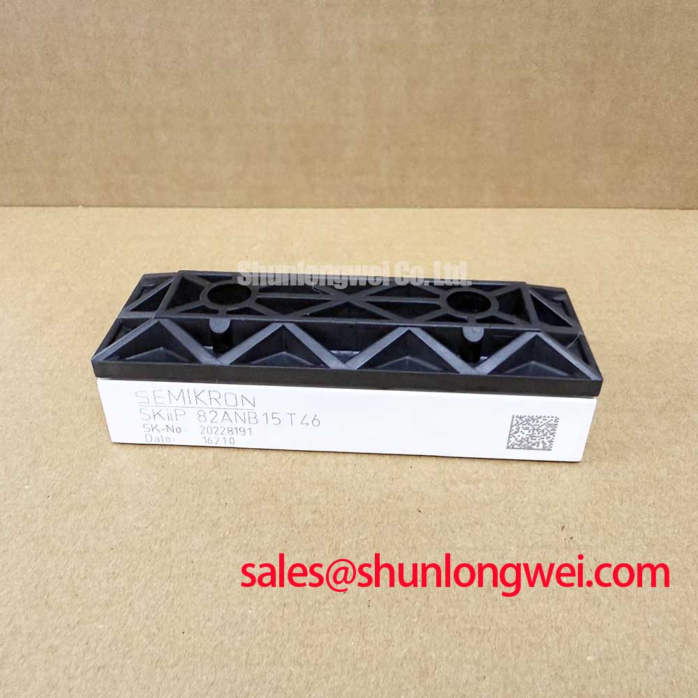
Before energizing a replacement, technicians should verify the nameplate voltage class, inspect the power terminals and insulation surfaces, and compare cold resistance readings with the known-good phase path. The SKIIP 83ANB15T4 is a Semikron CIB intelligent power module intended for evaluation in power conversion equipment such as heavy-duty variable frequency AC motor drives. Its official ratings include a 1200 V collector-emitter voltage and a 75 A nominal continuous collector current at Tcase = 25°C.
| Parameter | Official Specification |
|---|---|
| Manufacturer | Semikron |
| Product type | IPM with CIB topology |
| Collector-emitter voltage, VCES | 1200 V |
| Continuous collector current, IC, nom | 75 A at Tcase = 25°C |
| Collector-emitter saturation voltage, VCE(sat) | 1.9 V typical, 2.4 V maximum at IC = 75 A |
| Isolation voltage, Visol | 4000 V AC for 1 minute |
| Integrated functions | Gate driver, VCE(sat) protection and NTC temperature sensor |
The stated ratings define the component boundary, not the complete operating limit of a finished inverter. Switching frequency, DC-link voltage, motor-cable length, cooling conditions, gate-drive configuration and transient behavior must be checked at system level. The integrated gate driver, desaturation-related VCE(sat) protection and NTC temperature sensor can reduce external circuitry, but the original application documentation should still be checked before a replacement is commissioned.
When a drive uses a long motor cable, inspect the output waveform at the module terminals before judging the motor-end waveform. Cable inductance, termination impedance and the motor input network can create reflected waves. Under unfavorable conditions, the motor terminals may experience a transient approaching twice the incident voltage. This is a system-level transmission-line effect and should not be treated as an additional voltage rating of the SKIIP 83ANB15T4.
A practical commissioning sequence begins with a controlled low-energy test. Confirm the DC-link voltage, probe connection, grounding method and switching state, then capture the phase-to-phase and phase-to-earth waveforms at both the inverter output and the motor terminals. A ringing pattern that changes substantially with cable length or probe location may indicate impedance interaction rather than an immediate failure of the power module. Compare the result with the known-good drive topology and check whether the installed motor cable, shield termination and output reactor match the original machine configuration.
Design Consideration: Output filters, dv/dt filters and motor chokes should be selected from the measured switching waveform, motor insulation requirements and drive manufacturer limits. Their purpose is to control edge energy and reflected-wave amplitude without creating excessive current ripple or resonant interaction. The system designer should verify filter attenuation, thermal loading and phase balance during switching tests instead of applying a universal filter value.
Keep the commutation loop compact and separate high-current output conductors from sensitive control wiring. Maintain the clearance and creepage specified by the equipment insulation design, particularly around the DC-link and phase-output terminals. If a transient remains close to the 1200 V device boundary, do not infer suitability from the nominal DC-link value alone. Peak voltage, overshoot duration and repetitive switching stress require oscilloscope verification against the module and system documentation.
For a related Semikron MiniSKiiP reference point, engineers may compare the documented topology and electrical ratings of SKIIP37AC12T4V1. This is a reference for evaluation only; terminal arrangement, protection behavior and mechanical compatibility must be confirmed independently before any substitution is considered.
SKIIP 83ANB15T4 Thermal-Electrical Optimization: Galvanic Gate Drive Isolation, Reinforced Practical Tuning
The official data identifies a 4000 V AC isolation voltage for one minute. This is an isolation test rating and should not be rewritten as a guaranteed reinforced-insulation system rating for every assembled drive. The gate-driver barrier, PCB spacing, contamination environment, enclosure construction and safety architecture all affect the final isolation design. Engineers should consult the applicable Semikron documentation and verify the complete barrier with the equipment safety test plan.
Common-mode transient immunity is equally dependent on the gate-driver implementation and the power-loop layout. The supplied product data does not establish a CMTI value above 100 kV/µs for this specific unit. During commissioning, observe the gate-emitter waveform and the protection response while the inverter is switching at the intended DC-link voltage. Uncommanded gate movement, abnormal ringing or a protection event should be investigated by checking driver supply decoupling, return paths, probe technique and commutation-loop inductance.
Thermal evaluation should begin with the official loss-related voltage data: the VCE(sat) is 1.9 V typical and 2.4 V maximum at 75 A. Actual dissipation also depends on current waveform, conduction duty, switching losses, gate resistance, carrier frequency and junction-to-case thermal impedance. The 2 kHz to 16 kHz range can be used as an application test sweep when relevant to the drive, but it is not an official switching-frequency rating stated in the supplied product parameters.
At each test point, record case temperature, heat-sink temperature, airflow condition and phase-current balance. Higher carrier frequency generally increases switching loss, but the resulting temperature rise must be measured rather than estimated from frequency alone. Verify the NTC sensor against the drive controller’s configured scaling and fault thresholds, because an incorrect sensor interpretation can leave the thermal protection strategy ineffective.
For background on MiniSKiiP construction and integration topics, consult the Semikron MiniSKiiP Power Modules information and the Semikron-Danfoss SKiiP Technology reference. These manufacturer resources should be read alongside the exact product documentation for terminal definitions and protection behavior.
Field Diagnostics & Commissioning: Desaturation Protection in SKIIP 83ANB15T4 Topologies
The integrated VCE(sat) protection is relevant when the inverter experiences an abnormal current event, but the supplied parameters do not confirm a specific Type-I or Type-II desaturation classification, a sub-10 µs response time or a short-circuit safe operating area. Those values must be obtained from the applicable Semikron technical documentation before they are used in a protection calculation.
For field diagnosis, first isolate the event history from the drive controller. Determine whether the reported fault occurred during turn-on, steady conduction, commanded turn-off or an external short circuit. Then inspect the gate signal, driver supply, VCE response and phase-current waveform with appropriately rated differential probes. A protection trip without a visible current abnormality may involve false sensing, layout coupling, an unsuitable blanking arrangement or probe error; it should not be assigned to one cause without waveform evidence.
Two-stage soft turn-off is a possible system design approach for limiting the voltage rise associated with fault interruption. Its timing and gate-current profile must be coordinated with the module’s documented protection circuit and the stray inductance of the power loop. The design team should verify the resulting peak collector-emitter voltage against the 1200 V rating and measure whether the clearing sequence prevents repeated protection cycling.
Inspect the DC-link capacitor connection, busbar joints, phase terminals and snubber network after any high-energy fault. A loose connection can create additional inductive overshoot, while an incorrectly placed snubber may reduce effectiveness or increase circulating current. Keep the fault-current path physically distinct from logic and sensor wiring, and confirm that the NTC and protection feedback connections remain electrically secure after thermal cycling.
The Wide Bandgap Revolution reference provides broader context for switching-speed and layout trade-offs. It does not replace the Semikron data required to validate the protection timing of this silicon-based CIB IPM.
Field Diagnostics & Commissioning: Kelvin Emitter Connection in SKIIP 83ANB15T4 Topologies
Do not assume a Kelvin emitter terminal or a particular auxiliary-emitter pin arrangement from the product name alone. The official information supplied for the SKIIP 83ANB15T4 confirms the CIB topology and integrated gate-driver function, but it does not provide a complete terminal drawing. The system integrator should verify the exact pinout and mechanical layout from the applicable Semikron package documentation before routing the gate-driver return.
Where the documented interface provides a separate auxiliary emitter return, route that return directly to the driver reference and keep it separate from the high-current emitter path until the intended reference point. This reduces mutual coupling from di/dt in the power conductor and can improve the accuracy of gate-emitter voltage measurement. If the device drawing does not provide such a connection, do not create one by modifying terminals or assuming that a nearby power terminal has Kelvin behavior.
During commissioning, monitor gate-emitter voltage at the module interface, not only at the driver board. Compare turn-on and turn-off waveforms under no-load and representative motor-load conditions, then check for ringing that changes with probe placement or output-current direction. Excessive oscillation may involve common inductance, gate-loop routing, driver decoupling or an interaction with the motor cable, so the corrective action should follow measured evidence.
Use short, controlled gate and return paths, avoid routing them alongside fast phase-output conductors, and maintain the insulation spacing required by the equipment design. Check terminal torque and contact condition according to the original Semikron mechanical documentation. ⚠️ Maintenance Note: keep the heat sink and airflow path clean, and periodically compare contact temperature rise with the established commissioning baseline while checking for aged or displaced thermal interface material.
After maintenance, repeat insulation, phase-balance and low-energy switching checks before returning the drive to full load. The final acceptance decision should be based on the measured DC-link transient, gate waveform, protection response, case temperature and NTC feedback under the actual installation conditions.