

Content last revised on September 20, 2026
Field Diagnostics & Commissioning: High Frequency Commutation Loop Inductance in SKIIP 12NAB12T4V1 Topologies
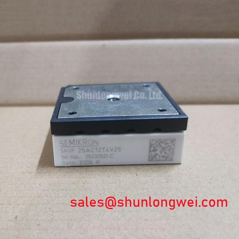
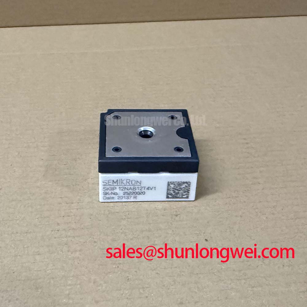
Begin commissioning by verifying the equipment nameplate against the module marking, then isolate the drive and inspect the MiniSKiiP / SKiiP housing, terminals, mating connector area, and thermal contact surfaces for handling damage, contamination, or distorted connections. SKIIP 12NAB12T4V1 is a Semikron IPM identified with an official 1200 V rated voltage and 12 A rated current. These values define the module’s documented electrical identity; the original equipment schematic and module documentation remain necessary to confirm terminal assignments, drive interface, protection behaviour, and the exact converter function in a repair assembly.
| Parameter | Value | Classification |
|---|---|---|
| Product model | SKIIP 12NAB12T4V1 | Official product identification |
| Manufacturer | Semikron | Official product identification |
| Rated voltage | 1200 V | Official Datasheet Specification |
| Rated current | 12 A | Official Datasheet Specification |
| Package family | MiniSKiiP / SKiiP | Official package information |
| Product category | Intelligent Power Module | Product classification |
Before applying DC link power, compare the installed busbar routing with the original assembly and inspect every connection in the high current commutation path. A loose laminated connection, a long return path, or an altered capacitor location can change switching behaviour even when the replacement module has the correct 1200 V and 12 A ratings. During turn off, peak voltage rises above the DC link level by an amount related to loop inductance and current transition rate. This is an Engineering Calculation relationship expressed by Vpeak being the DC link voltage plus parasitic inductance multiplied by di/dt.
A practical commissioning sequence is to begin with controlled low energy testing, observe collector or output voltage and current with appropriately rated differential measurement equipment, and compare waveforms with a known healthy drive where available. Ringing, unexpected overshoot, or irregular current transfer may indicate a layout issue, a decoupling path problem, or a gate drive interaction. They should not be attributed to the power module alone without measurement.
Design Consideration: keep the DC link capacitor connection and switching current return physically compact and geometrically symmetrical where the equipment architecture permits. Planar or laminated busbar arrangements are commonly evaluated because they can reduce loop area and help suppress inductive overshoot. Snubber capacitor selection, capacitor placement, and any clamp network must be verified at the actual switching current, DC link voltage, temperature, and control settings of the host equipment.
For equipment repair involving a precision stepper or BLDC motor servo motion actuator, inspect the encoder, control supply, current sensing path, and motor cable termination before concluding that a switching waveform is abnormal. Fast current commands and cable reflections can influence the observed waveform. The Semikron overview of MiniSKiiP power modules provides useful product family context when comparing mechanical integration constraints across an installed drive.
SKIIP 12NAB12T4V1 Operational Boundaries: Evaluating PCB Symmetry Considerations for Dual IGBT Limits
Verify terminal names and connection orientation from the original equipment documentation before installing SKIIP 12NAB12T4V1. Package family information alone does not establish the host converter topology, terminal function, gate drive arrangement, or auxiliary connection allocation. Continuity testing should be performed only with the system de energised and with sensitive control electronics protected from unintended test current.
In converter assemblies using separate power and control returns, mutual inductance in a shared emitter or return segment can feed switching noise back into the gate loop. Design Consideration: maintain a clearly defined low impedance driver return path and prevent high current power return routing from sharing avoidable impedance with gate reference connections. This principle helps reduce the conditions that can contribute to gate oscillation, false turn on, or inconsistent switching transitions.
Inspect PCB creepage and clearance around exposed power nodes after any repair, especially where replacement busbars, insulating sheets, standoffs, or cable ties have been fitted. Clearances must be assessed against the actual system voltage, pollution environment, enclosure design, and applicable equipment standard by the responsible system engineer. Do not infer insulation approval or EMC compliance from the module rating.
Mechanical restraint deserves equal attention. Busbars and connector interfaces should be secured so vibration cannot transfer cyclic force into module terminals or PCB solder joints. 💡 Pro Tip: Tighten busbar hardware in the equipment manufacturer’s specified sequence and recheck alignment before energising, because mechanical preload can change when adjacent connections are secured.
Where a repair review requires comparison with another Semikron family member, SKIIP37AC12T4V1 can be examined as a separate candidate, but interchangeability must be confirmed through pinout, control interface, electrical limits, thermal arrangement, and host drive documentation rather than model family similarity.
Transient Dynamics & Electrical Design: Negative Gate Bias vs Active Miller Clamp in SKIIP 12NAB12T4V1
Gate waveform inspection should focus on the relationship between the controlled switch command, the complementary switching node, and the driver reference. A rapid voltage transition at a power terminal can couple through internal capacitances into a nominally off gate. If the driver return path has impedance or the off state pull down path is inadequate, the measured gate voltage may move during the opposite device’s switching event. This behaviour may increase cross conduction risk, but the source can also involve probe grounding, controller timing, driver supply stability, or layout coupling.
Engineering Recommendation: assess whether the original gate driver uses a negative off state bias, an active Miller clamp, or another documented off state control method. A negative bias and an active clamp address the same broad concern through different circuit approaches. Their suitability depends on the driver architecture, isolation method, gate voltage limits, switching conditions, and protection timing specified for the complete equipment.
Keep the gate loop short, direct, and separated from high current switching conductors where possible. Gate resistor changes should not be made solely in response to audible noise, visible ringing, or a failed power device. Any change affects switching loss, voltage overshoot, diode recovery interaction, and control immunity, so it requires oscilloscope validation under controlled operating conditions.
The same caution applies to bootstrap and auxiliary driver supplies. Their capacitor recharge capability and diode recovery behaviour must be checked against the control timing and switching frequency used by the existing servo drive. A front end or auxiliary conversion stage using a device such as SKM100GB063D should be evaluated on its own documented ratings and topology, not assumed to be electrically interchangeable with this IPM.
Semikron describes the broader integration approach of its SKiiP technology. For repair personnel, the relevant practice is to validate the complete driver, sensing, protection, and power path as one system after module replacement.
Field Diagnostics & Commissioning: Baseplate Convexity Compensation and Screw in SKIIP 12NAB12T4V1 Topologies
Do not assume that every MiniSKiiP / SKiiP installation uses a baseplate, a screw mounted thermal interface, or a particular fastening method. Inspect the actual equipment assembly and follow its mechanical drawing. If the host system uses a heatsink interface, remove old interface residue carefully and check that the contact region is clean, flat, and free from raised burrs or trapped debris. Uneven contact can create local thermal stress and can complicate fault diagnosis after a repair.
Design Consideration: where the original mechanical design specifies thermal interface material, apply it as a controlled, uniform layer according to the equipment manufacturer’s process. The correct material type, thickness, compression behaviour, and fastener torque are installation specific and should not be inferred from the 1200 V, 12 A, or package family data. If screws are used, progressive tightening in the documented sequence helps avoid tilting a mounted assembly during compression.
After mechanical work, inspect connector engagement and route signal cables away from power busbars where the enclosure allows. Run a controlled functional test while observing heatsink temperature trend, current feedback consistency, fault reporting, and switching behaviour. A rising thermal trend may be associated with thermal contact, cooling flow, load conditions, switching operation, or sensing error; verify each path rather than treating temperature alone as a definitive failure signature.
For broader practical reference on evaluating industrial power semiconductor operating margins and repair testing, see Industrial Applications. High altitude operation, cosmic ray exposure, lifetime prediction, insulation reliability, and system EMC performance require equipment level assessment and applicable source documentation; no independent performance claim for SKIIP 12NAB12T4V1 should be inferred from this product page.