Content last revised on October 6, 2026
Transient Dynamics and Hard-Switching Checks for BSM200GAL120DLC
With the DC link isolated and discharged, check the installed module’s terminal markings and cold-state collector-to-emitter readings before removing it. Record the original wiring and mounting orientation so the replacement can be checked against the equipment schematic rather than against appearance alone. BSM200GAL120DLC is an Infineon IGBT module with a stated 1200 V voltage rating and 200 A current rating (Official Specification). Those ratings identify essential electrical boundaries, but they do not establish that the module fits a particular inverter, gate driver, or cooling assembly.
In a repair, the first switching question is whether the existing DC-link voltage and measured turn-off overshoot remain within the module’s 1200 V rating (Official Specification). The nameplate rating is not a substitute for a waveform measurement: busbar inductance and the rate of current change can raise the instantaneous collector-to-emitter voltage above the steady DC-link value. As a Design Consideration, keep the high-current commutation path compact and assess the resulting peak voltage under the equipment’s actual operating conditions. Probe placement matters; a long measurement ground lead can add a misleading spike to an otherwise useful trace.
Before energizing a replacement BSM200GAL120DLC, compare the driver connections, gate resistance network, protection input, and collector-to-emitter sensing path with the original circuit documentation. A desaturation signal can indicate that commanded conduction is not producing the expected low collector-to-emitter voltage, but its response depends on the driver, blanking arrangement, wiring, and fault conditions. The module’s supplied ratings do not specify a short-circuit withstand time, a detection deadline, or a mandatory shutdown sequence. Those limits must come from applicable manufacturer documentation and be validated in the finished power stage.
Two-stage soft turn-off is a possible driver-level Design Consideration when abrupt fault-current interruption would produce excessive inductive overvoltage. It should not be presented as a built-in feature of this module. Engineers assessing such a circuit should observe the fault-detection signal, gate waveform, and collector-to-emitter voltage together, then confirm that the chosen response protects the device without creating an unintended turn-on elsewhere in the bridge. For broader context on gate-drive and commutation-loop interactions, see IGBT Design & Integration.
If repeated trips occur only during load changes, retain the fault record and compare it with a measured switching event. A desaturation indication alone does not distinguish a genuine overcurrent from sensing noise, inadequate blanking, or a gate-drive problem. Check the signal path against the equipment schematic before changing protection settings.
Transient Thermal Impedance and Pulsed-Load Assessment
The 200 A rating (Official Specification) is a useful identity check, not permission to treat every pulsed load as a continuous or permissible operating condition. Junction temperature depends on conduction and switching losses, pulse duration, cooling conditions, and the thermal path into the heatsink. This distinction matters when evaluating an industrial inverter welder or medium-frequency induction-heating supply: either may impose a duty pattern that differs substantially from the conditions under which a headline current rating is specified. Compatibility should be determined from the original equipment requirements and the applicable full module datasheet.
For pulsed operation, transient thermal impedance is the relevant Design Consideration because the junction temperature can change faster than the heatsink temperature. If the manufacturer’s thermal-impedance curve or model is available, an engineer can apply the measured loss waveform to that model and compare the resulting peak junction estimate with the documented device limit. A multi-RC representation can help account for overlapping pulses, but fitting or using one without module-specific thermal data would turn an estimate into an unsupported specification. Avoid assigning a peak junction margin from the 200 A rating alone.
During inspection, look for uneven mounting contact, disturbed thermal compound, loose power connections, and signs of heating around terminals. These observations identify items to investigate; none proves a single cause of a prior trip. After assembly, compare case or heatsink temperature trends at repeatable load conditions while recording current and switching behavior. Temperature measurements taken away from the junction cannot, by themselves, establish the peak junction temperature during a brief overload.
A rising collector-to-emitter voltage during commanded conduction may support a protection diagnosis, but it also needs context from gate voltage, current, and temperature. Desaturation timing and soft turn-off are properties of the implemented driver and protection circuit, not additional published ratings established by the supplied BSM200GAL120DLC identification data. Verify their behavior against the installed driver documentation before using a fault trip to judge module health.
Assembly Integrity and Current-Path Layout
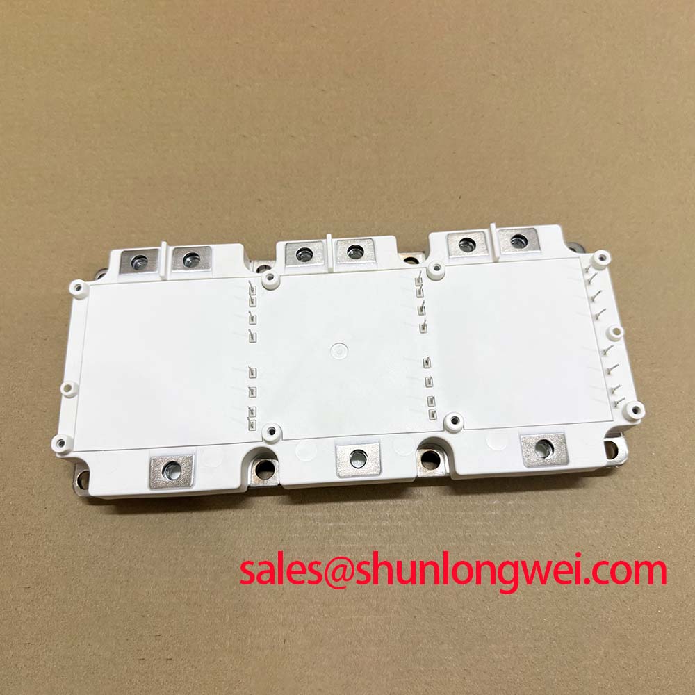
Check the module footprint, terminal locations, mounting surfaces, and connection hardware against the removed unit and equipment drawing before committing to installation. The package designation supplied for BSM200GAL120DLC is Module (Official Specification); it does not provide dimensions, terminal assignments, or fastening torque. Obtain those details from the applicable mechanical drawing. A visually similar housing is not enough to confirm that the busbar, control wiring, or heatsink interface will fit.
Static and dynamic current distribution require different checks if an equipment design uses devices in parallel. At steady state, sharing depends on the devices’ electrical characteristics and their thermal environment. A positive temperature coefficient of on-state voltage can assist sharing in some operating regions, but that behavior should not be assumed across all currents and temperatures without the relevant device curves. During switching, unequal gate-path impedance and unequal commutation-loop inductance can create a different imbalance even when static measurements appear similar.
As a Design Consideration, route parallel power paths and gate circuits with comparable geometry, then verify switching waveforms and device currents in the assembled equipment. Inspect bolted joints and the heatsink interface before interpreting a current imbalance as a semiconductor characteristic. Pro Tip: Keep paired commutation paths geometrically balanced, then confirm turn-off voltage peaks with switching tests rather than relying on visual symmetry.
A sourcing comparison also has to respect topology and rating differences. The linked BSM75GD120DLC is a separate part number to examine when reviewing related repair materials, not a confirmed drop-in replacement for BSM200GAL120DLC. Check its official circuit configuration, electrical ratings, pinout, and mechanical drawing against the equipment requirements before considering it for any position.
Operational Boundaries and Gate-Emitter Return Routing
Trace the gate-drive return to the actual emitter connection shown on the module’s verified terminal drawing. High current in a shared emitter conductor can develop a transient voltage that changes the gate-to-emitter voltage seen by the device. As a Design Consideration, minimizing shared impedance between the power-current path and the control return helps reduce unintended gate movement during fast switching. Do not assume this specific module provides an auxiliary Kelvin-emitter terminal unless its official pinout confirms one.
If a separate auxiliary emitter connection is documented, the driver return can be evaluated for connection to that terminal while the main emitter path carries load current. If it is not documented, the layout must be assessed using the terminals the device actually has. The objective is to limit coupling into the gate loop without inventing a connection or modifying the driver independently of the equipment schematic. Gate oscillation, false turn-on, and nuisance protection trips are possible symptoms of several circuit problems; compare measured gate-to-emitter and collector-to-emitter waveforms with a known-good signal path where one is available.
Gate routing is also where a module-level rating meets system-level protection. Review gate-driver isolation, the DC-link layout, sensing return, and shutdown behavior as one circuit, then determine clearance and insulation requirements from the equipment’s applicable design rules. The 1200 V device rating does not establish assembly clearance, insulation reliability, or EMC compliance. Infineon’s EconoDUAL™ 3 information offers context for examining module integration, but its product-family details should not be transferred to BSM200GAL120DLC without matching documentation.
For a repair evaluation, finish by measuring gate behavior during both turn-on and turn-off at the equipment’s intended operating points, while monitoring the DC link and collector-to-emitter voltage. If the protection circuit trips, preserve the timing relationship between those signals before changing components or settings. The system engineer can then assess voltage margin, switching stability, and thermal performance against the complete device documentation and the equipment’s own acceptance criteria.