


Content last revised on September 12, 2026
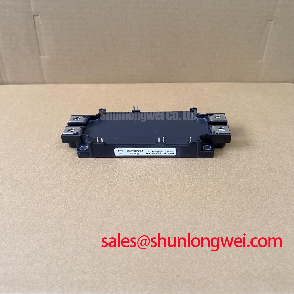
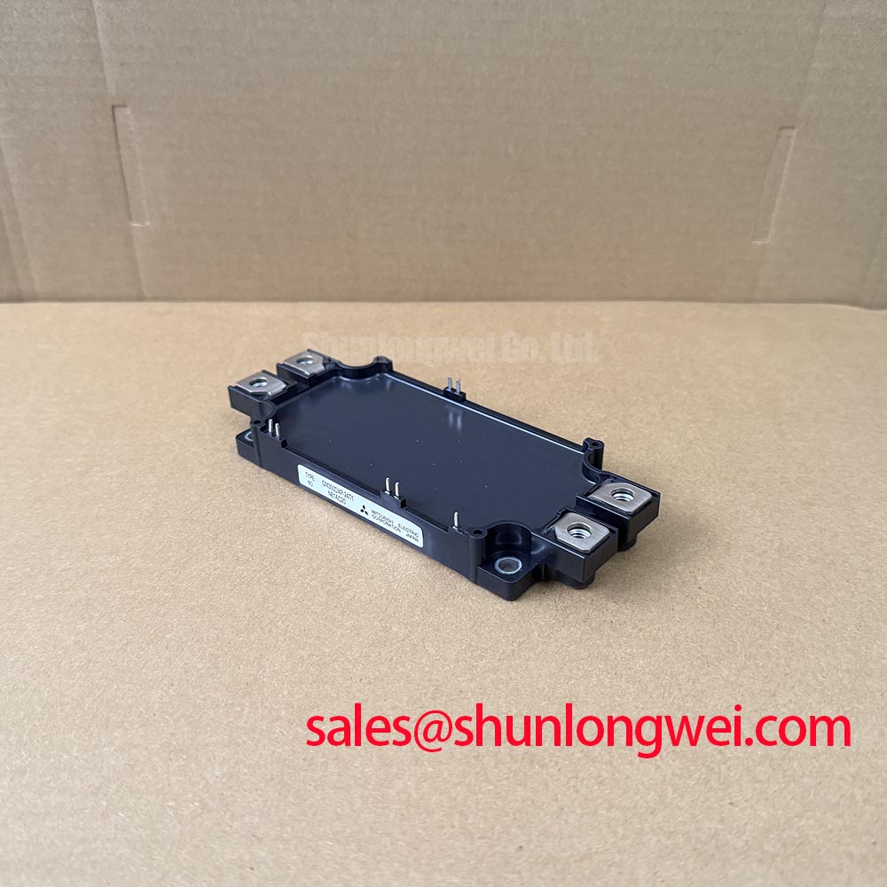
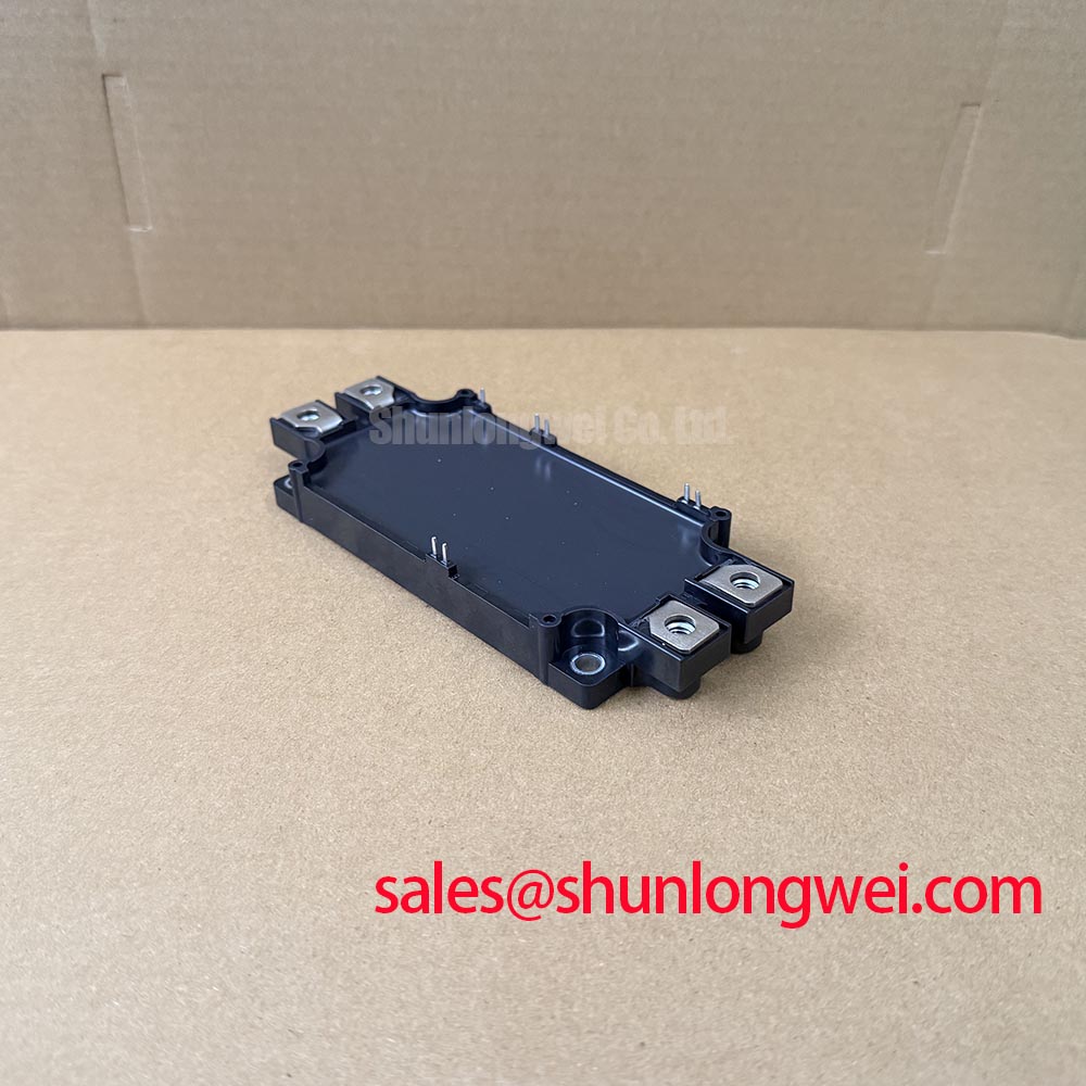
CM300DXP-24T1 Thermal-Electrical Optimization: Auxiliary Emitter Return Trace Separation Practical Tuning
| Manufacturer | Mitsubishi Electric |
|---|---|
| Part Number | CM300DXP-24T1 |
| Category | IGBT Module |
| Rated Voltage | 1200 V |
| Rated Current | 300 A |
| Package | Module |
| Topology | General Power Stage |
| Series | Standard |
With the module isolated, identify the main emitter and auxiliary emitter terminals from the original Mitsubishi Electric connection drawing, then compare each return path with the actual gate-drive wiring and oscilloscope reference point.
The CM300DXP-24T1 is specified as a 1200 V, 300 A Mitsubishi Electric IGBT Module in a module package, but its static rating does not by itself define the switching behavior of a complete inverter leg. A heavy-duty variable frequency AC motor drive can develop gate-loop disturbance when the high-current emitter return shares copper, vias, or connector impedance with the gate-driver reference. The resulting common impedance can shift the apparent emitter potential seen by the driver and may produce ringing, delayed turn-off, or an unexpected gate pulse.
As a Design Consideration, route the auxiliary emitter return directly to the gate-driver reference and keep the main power emitter return on its intended high-current path. The two paths should not be casually merged at a remote control-board ground point. Minimize the area of the gate-drive loop, keep the gate and auxiliary-emitter conductors physically paired where practical, and avoid routing them alongside the collector bus or braking-current conductor.
During commissioning, capture gate-to-emitter voltage at the module terminals rather than at the driver output alone. Compare the waveform during turn-on, turn-off, motor acceleration, and regenerative deceleration. If the driver waveform appears clean at its output but distorted at the module, investigate conductor inductance, connector contact resistance, auxiliary-emitter routing, and probe-loop pickup. A known-good phase leg provides a more useful reference than an assumed voltage threshold.
The official data supplied for this product identifies the voltage and current class, package, and general power-stage category. Gate charge, internal circuit arrangement, switching energy, transient thermal impedance, and terminal-specific electrical limits should be taken from the applicable manufacturer documentation before detailed loss or drive calculations. For a neutral comparison point within the same broad Mitsubishi Electric power-module field, engineers may review CM35MX-24A, while checking mechanical, electrical, and control compatibility independently.
💡 Bench Tip: Use ESD protection and record a cold-state diode-test baseline for each accessible power path before connecting the module to the drive, then compare the readings with a known-good unit under the same meter polarity.
CM300DXP-24T1 Circuit Protection & Reliability: Calibrating Galvanic Gate Drive Isolation, Reinforced
Measure the isolated driver output at the module-side gate and emitter reference while the power stage remains disabled, then verify that the measured common-mode behavior matches the isolation architecture selected by the system designer.
Reinforced galvanic isolation, common-mode transient immunity, and gate-driver supply behavior are system-level properties unless they are explicitly stated in the driver component documentation. The CM300DXP-24T1 product data provided here does not establish a guaranteed isolation withstand voltage or a guaranteed CMTI value for the complete gate-drive assembly. Those figures must not be assigned to the IGBT module itself.
As an Engineering Recommendation, inspect the isolation barrier, isolated power supply, driver return, gate resistor network, and control-board reference as one switching system. Confirm that the isolation device is rated for the working voltage, repetitive transients, pollution environment, and required reinforced insulation category. During a double-pulse or low-energy commissioning test, monitor the gate-to-emitter waveform and the isolated supply rails for disturbance that coincides with collector-voltage transitions.
Dead-time must be established from measured turn-off delay, device variation, driver propagation delay, temperature, and the intended switching conditions. It should not be copied from another module without verification. Complementary upper and lower switch commands require hardware interlock and a layout that prevents a control trace from coupling directly into the opposite gate channel. If a fault appears only during rapid voltage transitions, compare the isolated input waveform, isolated output waveform, gate-to-emitter voltage, and phase-leg current before assigning the fault to the IGBT module.
Gate-emitter protection is also dependent on the external circuit. The system integrator should verify the permitted gate-voltage range, negative turn-off bias requirements, clamp arrangement, and driver output capability from the relevant Mitsubishi Electric and gate-driver documentation. Negative bias can reduce susceptibility to unintended turn-on in some architectures, but excessive or poorly referenced negative bias can create its own stress and measurement errors.
For device-family background, the Mitsubishi Electric NX-Series IGBT Modules resource is useful for understanding manufacturer power-module terminology. It should be treated as technical background rather than as a substitute for the exact documentation applicable to this part number.
Preventing Spurious Faults: Baseplate Convexity Compensation and Screw Guidelines for CM300DXP-24T1
Inspect the mounting surface with the module removed, clean the contact area without scratching it, and look for uneven contact marks or displaced thermal-interface material after a controlled installation trial.
Thermal performance depends on the complete mechanical stack: heatsink flatness, baseplate contact, interface-material application, fastener sequence, clamping distribution, and the thermal duty cycle. The supplied product parameters confirm a module package but do not provide a manufacturer-approved interface thickness, baseplate flatness limit, screw torque, or mounting sequence for this page. Those values must come from the applicable mechanical drawing and installation instructions.
As a Design Consideration, apply only the interface material and coverage method specified for the actual heatsink and module combination. Excess material can increase thermal resistance, while insufficient coverage can leave dry areas beneath the baseplate. Air voids, contamination, burrs, and a tilted heatsink can create local thermal concentration even when the fasteners appear tight.
When the baseplate or heatsink shows measurable curvature, do not compensate by tightening one corner aggressively. Use the manufacturer’s permitted fastener pattern and tighten progressively so the contact pressure develops evenly. A crosswise sequence is a common mechanical practice, but the exact torque and sequence remain installation-document values rather than official electrical ratings of the CM300DXP-24T1.
After mounting, inspect the electrical insulation between the power terminals, control terminals, heatsink, and chassis according to the applicable safety procedure. Do not infer insulation quality from a simple continuity check. The correct test voltage, ramp, duration, discharge method, and acceptance criterion are determined by the equipment insulation design and the component documentation.
For thermal commissioning, use the measured case temperature, switching frequency, load profile, and cooling conditions to build the system’s transient thermal-resistance model. The pulse peak junction-temperature margin must be calculated from manufacturer thermal data and validated with an appropriate measurement method. If a thermal trip occurs during short acceleration or braking events, compare the event waveform with the calculated transient response rather than relying only on steady-state case temperature.
High-altitude operation and cosmic-ray-related single-event effects may require a separate reliability assessment for high-voltage power semiconductors. No FIT, SEB rate, operating-life figure, or altitude derating value is established by the supplied specifications for this product, so those values should not be invented. The broader principles of gate-drive layout, thermal management, and power-stage verification are discussed in IGBT Design & Integration.
Field Diagnostics & Commissioning: Overvoltage Trip Prevention via Fast-Switching in CM300DXP-24T1 Topologies
Capture the DC-link voltage, collector-emitter voltage, gate-to-emitter voltage, and phase current at the module terminals during the first controlled deceleration test, with the probe reference arranged to avoid a long measurement loop.
An overvoltage trip during motor braking can involve DC-link capacitance, regeneration control, braking-command timing, busbar inductance, stray inductance, snubber behavior, current measurement delay, or the external braking path. The 1200 V rating of the CM300DXP-24T1 is an official product specification, not a permission to operate the complete drive at that voltage without transient margin. Peak collector-emitter voltage must be checked against the actual switching waveform and the limits stated in the applicable device documentation.
For a heavy-duty variable frequency AC motor drive, the braking IGBT and ballast resistor are system-selected according to motor inertia, deceleration profile, DC-link voltage, duty cycle, resistor pulse capability, cooling, and braking-controller response. The module data supplied here does not confirm an internal braking transistor or define a compatible resistor. Designers should verify whether the required braking function is implemented by this power stage, an external chopper, or a separate module.
During fault tracing, first separate a genuine regenerative overvoltage from a measurement artifact. Use suitable differential voltage probes, check probe compensation, compare the captured signal with the DC-link sensor, and inspect whether the trip timestamp aligns with current decay or gate-command changes. A sharp transient that appears on only one probe channel may indicate probe placement or common-mode pickup rather than a semiconductor failure.
Minimize the commutation-loop inductance and keep the high-current braking path physically compact to reduce turn-off overshoot. The required layout clearance, snubber selection, gate resistance, and switching speed must be determined through switching tests using the actual bus voltage, load current, temperature, and mechanical assembly. If the waveform approaches the device boundary, reduce switching stress through a verified system adjustment and repeat the test across the intended operating range.
When a module is suspected after an overvoltage event, disconnect it from the energized circuit and perform a controlled static comparison of the power terminals and gate-emitter paths. A diode-test result can help identify an obvious short or open condition, but it cannot prove dynamic switching health, insulation reliability, or the absence of latent damage. The Mitsubishi Electric SiC Power Modules and SBDs resource may assist with technology comparisons, but any substitution decision requires independent voltage, current, gate-drive, thermal, mechanical, and protection verification.