Content last revised on October 16, 2026
Benchtop Waveform Tuning: Mitigating Stress via Galvanic Gate Drive Isolation for CM75DY-24H
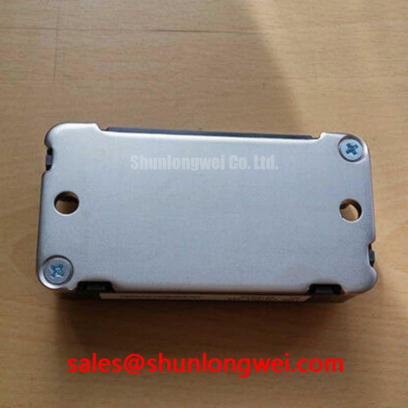
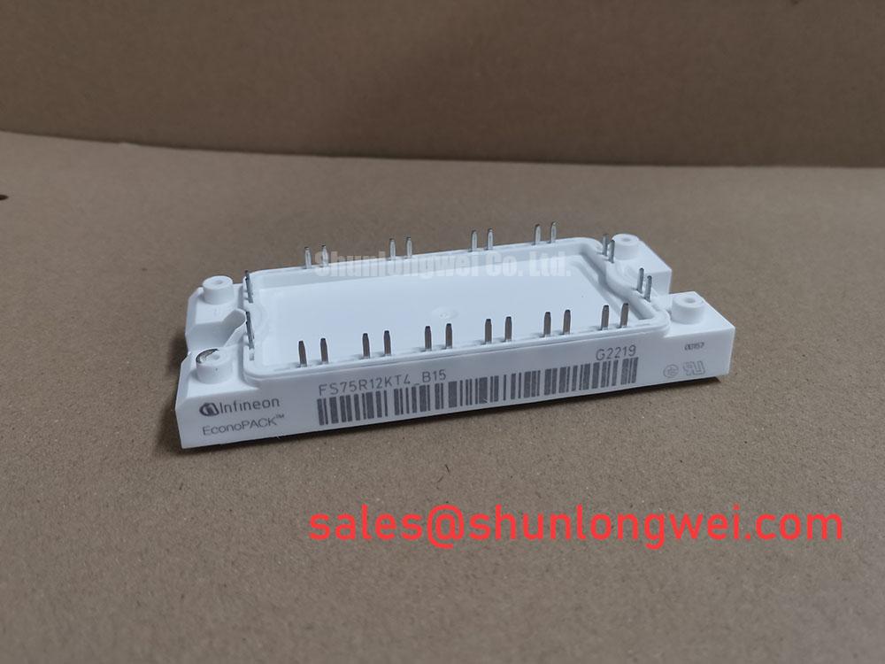
With the inverter welder isolated and the DC link fully discharged, inspect the power module terminals for discoloration, looseness, and contamination before applying any bench signal. The replacement under evaluation is the CM75DY-24H from Mitsubishi Electric, a 1200 V, 75 A IGBT Module.
Those ratings establish the component identity and its principal electrical boundary, but they do not replace the switching, transient, thermal, or insulation checks required by the host circuit. For industrial inverter welders and medium frequency induction heating supplies, compare the original gate wiring, busbar arrangement, cooling path, and protection network before energizing a replacement. Mitsubishi Electric’s Power Semiconductors and High Power Modules resource is a suitable manufacturer reference for device family and application context.
Start waveform work at the gate-drive boundary, not at the power terminals. The isolation barrier between the controller and the switching stage should be checked for reinforced insulation where required, with the system design reviewed against its intended working voltage, pollution environment, and safety architecture. An isolation withstand test target above 5 kV and a common-mode transient immunity target above 100 kV/µs may be used as design review criteria where the drive circuit demands them; these values are Design Considerations, not official CM75DY-24H ratings. A withstand voltage alone does not establish reinforced insulation; the applicable standard, test waveform, duration, and working-voltage requirements must also be satisfied.
Use a differential probe suitable for the switching node and a properly isolated probe arrangement for the gate emitter reference. Observe the gate signal during turn-on, turn-off, diode recovery, and sudden load changes. A narrow unwanted pulse on the gate can result from inadequate common-mode immunity, excessive parasitic coupling, probe reference error, or an unstable isolated power supply. Confirm the observation with a known-good drive channel before changing the gate resistor.
Keep the isolated driver loop compact and route the gate and return conductors as a closely coupled pair. The power commutation loop should remain physically separated from the controller signal path, while the isolation barrier maintains the required creepage and clearance for the actual working environment. Designers should verify the board spacing against the applicable insulation standard, pollution degree, altitude, coating method, and enclosure condition rather than applying a universal distance to every installation.
When a spurious gate pulse appears only during high-current switching, reduce the measurement loop first and then inspect the driver supply decoupling, return reference, and common-mode current path. A gate waveform that looks clean at low bus voltage but becomes distorted during normal operation points toward a dynamic coupling problem that requires oscilloscope correlation with collector-emitter voltage and current. The UM100CDY-10 may also be reviewed as a separate power-device reference, without assuming application compatibility or electrical interchangeability.
⚠️ Maintenance Note: De-energize and verify the DC-link discharge before connecting or removing any gate-drive cable, because an apparently inactive inverter can retain hazardous stored energy.
CM75DY-24H Operational Boundaries: Insulation Screening and Inspection
Insulation screening should be performed with the module disconnected from the control electronics and the test instrument configured for the applicable manufacturer-approved maintenance procedure. Use the test voltage, duration, terminal connections, and acceptance criteria specified for the module and equipment insulation system rather than applying a generic high-voltage test. The result should be recorded against the module temperature, humidity, test duration, and connection arrangement.
Changes in insulation resistance between a clean, dry inspection and a later test can justify a closer examination of the ceramic substrate region, mounting surface, terminal contamination, and creepage path. Do not interpret one reading as proof of a specific internal failure mode. Repeat the measurement with controlled lead placement, inspect the baseplate and mounting interface, and compare the result with the original equipment maintenance record when available.
Industrial airborne dust can create a conductive film across external insulation paths, particularly where cooling airflow carries metallic particles or welding residue. Remove contamination using a process approved for the assembly and environment, then allow the module and heatsink area to stabilize before retesting. The clearance path should remain free of burrs, loose hardware, cable strands, and deposits that could bridge an insulation surface.
High-side gate power deserves separate attention in half-bridge and bootstrap arrangements. The bootstrap capacitor must support the gate charge demanded during the intended on-time while also supplying driver quiescent current and leakage, with allowance for temperature variation and refresh requirements. Select its capacitance from the driver and switching sequence, then verify the high-side supply waveform under the actual duty cycle. The capacitor value is a system design result, not a fixed characteristic of the CM75DY-24H.
For service work on a bidirectional DC to DC battery charger, monitor the thermal pattern in both charging and regenerative discharging directions. Repeated heat cycling can alter interface pressure, compound condition, and terminal contact quality. A maintenance record should correlate heatsink temperature, airflow condition, switching duty, and fault history rather than relying only on the 75 A nominal rating.
Assembly Integrity and Layout Architecture: Evaluating Diode Recovery Stress for CM75DY-24H
Evaluate the antiparallel diode and commutation path with a current probe and a voltage probe positioned at the module terminals. The engineering question is whether reverse recovery current and its rate of change are producing excessive voltage ringing, gate disturbance, or electromagnetic emission. The CM75DY-24H listing supplies the 1200 V and 75 A ratings, but no diode softness factor, peak reverse recovery current, or recovery waveform values are provided here; those quantities must be taken from the applicable device documentation or measured on the installed circuit.
Recovery-related stress can be intensified by long bus connections, uneven current sharing, or a turn-on gate resistance that is too aggressive for the commutation loop. Long probe leads can also exaggerate apparent ringing. Begin by validating the measurement bandwidth and probe placement. Then compare the current slope and collector-emitter voltage across a controlled range of gate-drive conditions. If the ringing follows the gate transition, a carefully selected turn-on damping network may be evaluated. If it remains when the gate transition is unchanged, the busbar and commutation geometry deserve priority.
RC snubber selection should follow measured energy, ringing frequency, capacitor pulse capability, resistor loss, and the available thermal path. This is an Engineering Recommendation, not a preset value for this module. The snubber must be mounted close to the electrical loop it is intended to control; placing it remotely on a control board can add the same parasitic inductance that caused the original overshoot.
Use symmetrical planar conductors where the topology permits, keep the high di/dt loop compact, and separate the gate return from the power return until the intended reference point. Clearance should be reviewed around the high-voltage terminals, snubber components, heatsink hardware, and conductive enclosure parts. In an inverter welder, check the cable path to the transformer or output rectifier because a mechanically convenient cable route can become part of the transient loop.
For medium-frequency induction heating equipment, inspect the complete resonant power path rather than attributing a hot terminal to the module alone. Poor bus contact, loosened laminated conductors, cooling obstruction, and altered load tuning can all change the observed recovery stress. When comparing a possible higher-current family member such as CM300DY-24A, engineers should compare topology, voltage class, gate requirements, thermal impedance, mechanical fit, and protection coordination instead of treating current rating as a direct substitution rule.
CM75DY-24H Circuit Protection and Reliability: Calibrating Turn-Off di/dt Induced Vpeak Clamping
Turn-off protection should be calibrated from the measured DC-link voltage, switching current, commutation-loop inductance, and current fall time. The transient relationship can be described in the measurement narrative as the collector-emitter voltage exceeding the DC-link voltage by the inductive term associated with loop inductance and current slew rate. This makes clear why a 1200 V rating alone cannot establish a safe switching waveform. The system engineer must verify the measured peak against the device’s applicable transient and switching limits.
Use a low-inductance differential measurement arrangement directly across the power terminals and repeat the test at the operating temperature that produces the most demanding switching behavior. Compare turn-off overshoot with the gate voltage, current trace, and protection trigger timing. If the clamp activates inconsistently, investigate sensing delay, wiring inductance, clamp placement, and driver timing before increasing the clamp threshold.
Snubber capacitors and clamp components should be selected from measured transient energy, repetition rate, voltage stress, pulse current, and thermal dissipation. Their placement should preserve a short, symmetric path around the switching devices. A fixed layout target such as a particular nanohenry value should not be adopted without a validated parasitic extraction and switching measurement; the acceptable loop inductance is determined by the actual bus construction and the required voltage margin.
For regenerative braking choppers, examine the full energy absorption path through the braking resistor, switching device, clamp, resistor contactor, and cooling system. A resistor that is correctly rated for average power can still create severe instantaneous electrical stress if the chopper timing or DC-link rise is abnormal. Review the braking command, resistor temperature, fan or duct condition, and overvoltage trip record together.
In a battery charger with repeated charge and discharge cycles, thermal recovery between switching events should be evaluated alongside peak temperature. The relevant maintenance evidence includes heatsink temperature rise, airflow condition, interface material condition, terminal torque history, and the stability of the gate waveform after the equipment reaches operating temperature. Do not use the 75 A value as a substitute for an application-specific RMS current, pulse current, or transient thermal calculation.
The 1200 V CoolSiC™ MOSFET reference can provide a useful comparison point when reviewing high-voltage switching behavior and busbar practice, but a different semiconductor technology should not be treated as a drop-in replacement for this IGBT module. Final protection coordination remains dependent on the original converter topology, driver behavior, cooling assembly, and verified switching waveforms. Mitsubishi Electric’s Global Semiconductor Device Technologies resource may be consulted for broader manufacturer technology context.