“This article focuses on one of the most important architectural features of the new continuous-time sigma-delta (CTSD) precision ADC: easily driving resistive inputs and references. The key to achieving the best signal chain performance is to ensure that the input source or reference itself is not corrupted when it interfaces with the ADC. When using traditional ADCs, a complex signal conditioning Circuit design—called a front-end design—is required to seamlessly interface the input and reference to the ADC. The unique architectural features of CTSD ADCs simplify and innovate the interface of such ADCs to inputs and references. First, let’s quickly review the front-end design of a traditional ADC.
“
By Abhilasha Kawle and Roberto Maurino, Analog Devices
This article focuses on one of the most important architectural features of the new continuous-time sigma-delta (CTSD) precision ADC: easily driving resistive inputs and references. The key to achieving the best signal chain performance is to ensure that the input source or reference itself is not corrupted when it interfaces with the ADC. When using traditional ADCs, a complex signal conditioning circuit design—called a front-end design—is required to seamlessly interface the input and reference to the ADC. The unique architectural features of CTSD ADCs simplify and innovate the interface of such ADCs to inputs and references. First, let’s quickly review the front-end design of a traditional ADC.
Front-end design of traditional ADC
In this article, “sensor” and “input signal” are used interchangeably to represent any type of voltage input to an ADC signal chain. The input signal to the ADC signal chain can be a sensor, a signal from some source, or a feedback from a control loop. It is well known that in traditional discrete-time sigma-delta (DTSD) ADCs and successive approximation register (SAR) ADCs, the sampling networks at the input and reference are switched capacitor loads. When the switch is on, the capacitor charges the input; when the switch is off, the capacitor holds the sampled value. At each sample clock edge, when the switch reconnects the capacitor to the input, a finite current (called kickback current) is required to charge or discharge the capacitor to the new sampled value. The curve of this current is shown in Fig. 1a. Most sensor and reference ICs cannot drive kickback currents of this magnitude, and there is a high chance of corruption of the input signal or reference if interfaced directly with the ADC. One of the known solutions to avoid this corruption is to use a drive buffer amplifier to isolate the input sensor and reference from the ADC. The driver amplifier should have the ability to absorb this kickback current, as shown in Figure 1b. This results in the need for a high slew rate and high bandwidth amplifier to support the required input charge/discharge current and allow the kickback to settle within one sample time period. These stringent requirements limit the choice of buffer amplifiers that can be used in the input and reference paths of traditional ADCs.
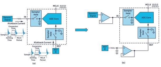
Figure 1. (a) Kickback current at the input and reference of a traditional ADC, (b) The kickback current is isolated from the input and reference by a buffer
On the other hand, a low-pass anti-aliasing filter is required at the input to ensure that high-frequency noise and interfering signals are attenuated significantly so that when they are folded back due to sampling of the frequency band of interest, performance is not degraded. The challenge facing ADC signal chain designers today is to fine-tune the competing requirements—alias suppression and output stability. The front-end design of the DTSD ADC using the driver and anti-aliasing filter is shown in Figure 2.
The input path consists of an instrumentation amplifier (in-amp) that interfaces the sensor with a fully differential amplifier (FDA) that ultimately drives the ADC. The instrumentation amplifier isolates the input sensor environment from the ADC circuitry. For example, the common-mode (CM) signal of a sensor can be very high (up to tens of volts), but most FDAs and ADCs do not support such high input common-mode voltages. Typical instrumentation amplifiers are capable of supporting wide input common-mode voltages while providing output common-mode voltages suitable for FDA and ADC. Another advantage of instrumentation amplifiers is their high input impedance. This means that if the sensor cannot directly drive the FDA’s input resistance, the sensor can interface with the FDA through an instrumentation amplifier. The FDA itself needs to have high bandwidth and high slew rate for the output to settle faster. Active anti-aliasing filters (AAFs) need to be built around the FDA in order to suppress interfering signals.
The requirements for the driver of the input or voltage reference are conflicting: on the one hand, fast settling requires high bandwidth, but on the other hand, filtering of noise and interfering signals requires low bandwidth. On the reference path, the front-end design of the DTSD ADC signal chain is shown in Figure 2. The reference IC is connected to a buffer that drives the ADC’s reference load. There is also a noise filter in the design to cut off the noise of the reference IC and buffer above a certain frequency. The design requirements for this filter are discussed later. Reference buffers have high bandwidth and high slew rate requirements to more quickly smooth out sampling event disturbances.
Part 1 of this article series has shown that a new signal chain using a precision CTSD ADC can be 68% smaller than the complex signal chain of a traditional ADC. This size reduction reduces BOM, and the simple design helps signal chain designers get to market faster.
Advantages of CTSD ADCs: Positive Inputs and References
Part 2 explains the CTSD ADC architecture to the signal chain designer, an unconventional approach to inverting a closed-loop amplifier. As discussed in Part 2, a CTSD ADC can be thought of as a Sigma-Delta ADC with a resistive input and reference load. The input and reference structures are simple resistive loads, which means there are no high bandwidth or high slew rate drive requirements. Section 3 demonstrates the unique advantages of CTSD, its inherent aliasing suppression capability against interference. In traditional signal chain designs, external alias suppression filters are required to attenuate interfering signals, which is an additional challenge, but CTSD ADCs do not require an external AAF. Due to the inherent aliasing suppression characteristics of CTSD ADCs, the signal transfer function of the modulator loop is equal to that of the antialiasing filter that attenuates high frequency interference. Due to the resistive input and inherent AAF, the input network is simplified and the sensor can be directly connected to the ADC. In situations where the sensor does not have the capability to drive this resistive load, an instrumentation amplifier can be used to interface the sensor with the ADC. Similarly, on the reference side, a reference buffer is not required in the CTSD ADC signal chain due to the resistive load. Figure 3b shows a simplified schematic using an instrumentation amplifier.
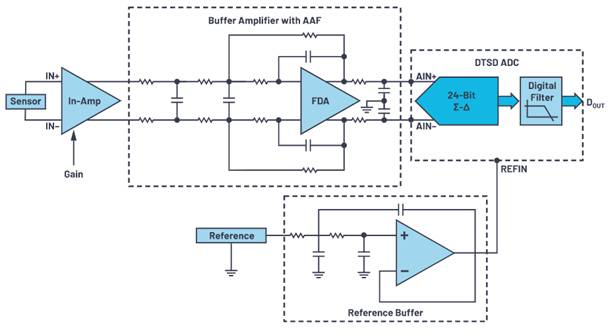
Figure 2. Front-end design of a discrete-time Sigma-Delta ADC

Figure 3. (a) CTSD architecture provides resistive input and reference load, (b) Direct instrumentation amplifier and reference drive CTSD ADC
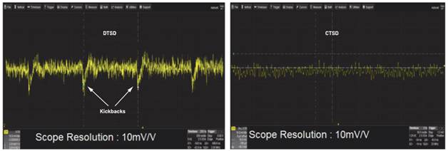
Figure 4. (a) Kickback in input current for DTSD ADC, (b) Continuous input current curve for CTSD ADC
Figure 4 shows further support for how CTSD ADCs can help simplify input front-end designs. For DTSD ADCs, the discontinuity in the input current due to kickback can be clearly seen when the input sampling switch changes state. For CTSD ADCs, it can be observed that the input current is continuous, which maintains signal continuity.
Simplify input-driven design
We have shown that the input drive of the CTSD ADC is resistive. This section will explain how to determine the input impedance R when planning the input drive of the ADCINvalue of . RINis a function of the ADC’s rated noise performance. For example, the AD4134 is a precision CTSD ADC with a dynamic range of 108 dB and a 4 V reference with an input impedance of 6 kΩ differential. This shows that when a full-scale 8 V pp differential input signal is applied, the peak current requirement is 1.3 mA pp. If the sensor can support the input current VIN/RIN, it can interface directly with the ADC. Scenarios that require a simple amplifier to drive such a resistive load are:
1. The sensor does not have the required drive capability to provide VIN/RINthe peak current.
2. The signal chain design requires either gain or attenuation for the sensor output.
3. Isolate the input sensor environment from the ADC circuit.
4. The sensor has a large output impedance.
5. The sensor is far from the ADC, and the track routing may add considerable resistance to the input.
In scenarios 4 and 5, the additional external resistor RSThere will be a voltage drop that represents a loss of signal at the ADC input. This results in gain error and error drift over temperature in the signal chain, resulting in degraded performance. The temperature drift of the gain is caused by the different temperature coefficients of the external and internal resistances. Using a simple amplifier to isolate the extra external resistor can solve this problem. Since the driving load of this amplifier is resistive, the selection criteria for this amplifier are:
• Input Impedance: To avoid signal attenuation or loss, the impedance of the sensor should match the amplifier input impedance.
• Output Impedance: The output impedance should be sufficient to drive the resistive input load of the ADC.
• Output Type: As a general signal chain design guideline, a differential signaling strategy is recommended for optimal signal chain performance. Design techniques for differential output type amplifiers or single-ended to differential outputs are best suited for this task. Also, for best performance, it is best to set the common mode of this differential signal to VREF/2.
• Programmable gain: The input signal is typically amplified or attenuated to map it to the full-scale range of the ADC. This is because the highest performance can be obtained from the ADC signal chain when the full-scale input range of the ADC is used.
Depending on the application, the amplifier can be an instrumentation amplifier or FDA, or a combination of two single-ended op amps — forming a differential output amplifier. There are no hard requirements for high slew rate or high bandwidth, and the CTSD ADC can be driven by choosing from ADI’s broad portfolio of amplifiers based on application needs. In addition, amplifier performance parameters are typically specified with resistive loads, which makes selection easier.
For example, for the AD4134, a performance-compatible instrumentation amplifier choice with programmable gain options and fully differential outputs is the LTC6373. This instrumentation amplifier provides high impedance to the input source and can easily drive differential 6 kΩ impedances with noise and linearity performance comparable to ADCs. With its extensive input common mode support and programmable gain options, any sensor or input signal with a wide range of signal amplitudes can be interfaced with the ADC. An example of an input front-end design using this direct instrumentation amplifier drive is shown in Figure 4.
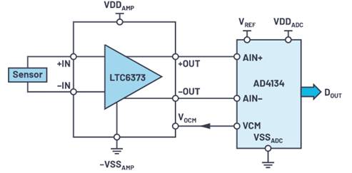
Figure 5. Input Front-End Design, CTSD ADC Directly Interfaced with Instrumentation Amplifier
Another example is a simple low-voltage front-end design using a fully differential driver amplifier such as the LTC6363-0.5/LTC6363-1/LTC6363-2, based on the desired gain or attenuation, as shown in Figure 6. Scenarios where the FDA can be used are when the sensor has the capability to drive the resistive load of the FDA, but is a single-ended type or has a common mode that the ADC does not support, or when the signal chain requires small gain/attenuation.
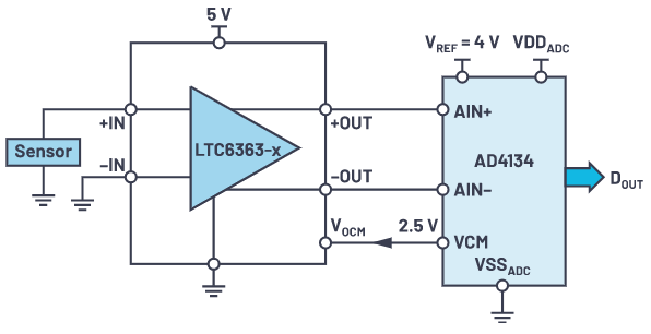
Figure 6. Input Front-End Design, CTSD ADC Directly Interfaced with Fully Differential Amplifier
Another example is a low-BOM scheme that uses two single-ended op amps to convert the single-ended input to a fully differential signal to the ADC, as shown in Figure 7.
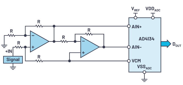
Figure 7. Input Front-End Design, CTSD ADC Using Two Single-Ended Amplifiers
There are many other examples like using a combination of single-ended instrumentation amplifiers and single-ended op amps to build differential output front ends to support very high input common mode or low drive strength single-ended sensors. Any such combination can be chosen based on performance, area and BOM requirements to better suit the application.
Other amplifiers compatible with the AD4134 are:
• Operational amplifiers ADA4625-2, ADA4610-2, AD8605, and ADA4075-2.
• Fully Differential Amplifiers: ADA4940-2, LTC6363, and ADA4945-1.
• Instrumentation Amplifier: AD8421.
The ADI Amplifier Selection Guide can be used to select the best amplifier for a specific application. For example, for high linearity applications such as audio test equipment, the ADA4945-1 is recommended. For photodiode applications where very high input impedance is the most important consideration, a transimpedance amplifier (TIA) such as the ADA4610-2 can be used.
The CTSD ADC greatly simplifies the input front end, and then we look at a similar simplification in reference driving.
Simplify Reference Design
The ADC output is a representation of its input and reference, as shown in Equation 1.

where VIN = input voltage level, VREFADC = ADC reference voltage, N = number of bits, and DOUT = ADC digital output.
Equation 1 shows that for optimum ADC performance, a clean and intact reference is important. There are three main performance indicators of ADCs that are affected by reference voltage errors:
Signal-to-Noise Ratio (SNR): The main sources of noise contributing to SNR are the input path, the ADC itself, and the voltage reference. For the total noise of interest at the ADC output, the reference noise budget is typically 1/3 or 1/4 of the output noise of the stand-alone ADC, taking into account other noise sources. References or reference buffers typically have higher noise than ADCs. In the data sheet of a reference or reference buffer IC, one can see the spectral noise density or Noisedensityis one of the technical specifications. Recalling the noise calculation basics, the total noise at the output of the reference or reference buffer is given by:
![]()
We have no control over Noisedensity, as it is fixed for the selected reference or buffer. The only controllable parameter is the noise bandwidth (NBW). To reduce reference noise, we need to reduce the noise bandwidth of the reference or reference buffer. This is typically accomplished by connecting a first-order low-pass RC filter to the ADC, as shown in Figure 8. For a first-order RC filter, NBW is given by:

• ADC reference current I flowing through filter resistor RADCCauses a voltage drop, which changes the actual reference voltage value of the ADC. Therefore, it is recommended to choose a small value of R and a large value of C to meet the NBW requirement of low reference noise.
• Gain Error: As can be seen from Equation 1, VREFADCDetermines the slope of the output-to-input transfer function, as in a line equation like y = mx. This slope is also known as the gain of the ADC. Therefore, if the reference voltage source changes, the gain of the ADC will also change.
• Linearity: For traditional DTSD ADCs and SAR ADCs, the reference current and accompanying kickback are input signal dependent. Therefore, if the reference is not fully settled before the next sample clock edge, errors on the reference will be input dependent and cause nonlinearity. Mathematically, VREFADCcan be expressed as
Referring to Equation 1, based on ADC input, ADC output DOUTThere will be various higher-order dependencies that cause harmonics and integral nonlinearity.Therefore, traditional ADCs rigidly require reference buffers with high slew rate and bandwidth to allow the reference output to settle over the sample time period
If we analyze SNR and linearity carefully, we see that the reference or reference buffer has conflicting requirements to meet. Low noise requires low bandwidth, but fast settling requires high bandwidth. Properly balancing these two requirements has long been a challenge for signal chain designers. Some of the latest DTSD ADCs and SAR ADCs incorporate reference buffers on-chip to simplify one step in the signal chain design, but these solutions require additional power or compromise performance to some extent. CTSD ADCs do not require fast settling buffers, nor do their resistive inputs require fast settling drivers, thus avoiding performance issues.
CTSD ADCs address reference driver challenges with the following features and design improvements:
The reference is a resistive load and has no settling requirements on each sample clock edge. Therefore, designers can connect the reference IC directly to the ADC without the need for a dedicated reference buffer.
A patented design technique makes the reference current independent of the input and forces the ADC’s reference current IADCremained basically constant. This is beneficial when an RC filter may be required to reduce reference noise, as shown in Figure 8. The result is a constant voltage drop across the resistor with no input dependent term added to VREFADCsuperior. We have designed a measure to digitally correct the system-level gain error based on the value of R and the voltage measured at the reference pin. Therefore, this simple reference interface has no gain or linearity errors.
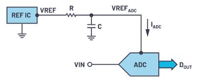
Figure 8. Resistive Reference Load Enables Direct Connection of Reference IC to Passive Filters
Although steps have been taken to digitally correct the error due to the voltage drop across R, one might ask whether this would limit the full-scale range of the CTSD ADC because the ADC’s actual reference voltage (VREFADC) will be less than the applied VREF.
For example, if the VREF of the reference IC is adjusted and set to 4.096 V, the ADC reference current (IADC) = 6 mA, then, for a filter resistor of R = 20Ω, the actual reference voltage of the ADC (VREFADC) is 3.967 V, as shown in Equation 5. In this case, when 2×VREF = 8.192 V pp is applied at the ADC input (which is greater than 2×VREFADC), is it possible to saturate the ADC output with a rated full-scale differential input? The answer is “no”. CTSD ADCs are designed to support input amplitudes that exceed the reference voltage at ADC pin REFIN by a few mV. In our AD4134 example, this extended range limits the resistance value to a maximum of 25Ω. The value of C for the noise filter is then chosen to satisfy the calculated noise bandwidth.
Simplifies Reference Drive Designs
The CTSD ADC simplifies the design of the reference drive, but there are other factors to consider when choosing the correct R for the filter and then digital gain error correction for the voltage drop across the resistor. Digital gain error correction (also known as calibration) is a common feature of many ADCs and gives the signal chain designer the freedom to compensate for errors in the signal chain at the digital output of the ADC. Therefore, it may not require additional design steps but reuse the same algorithm, which is common for many signal chains. In this case, the choice of resistors does not seem to be a special design step, but there is one caveat: the temperature dependence of the voltage drop. External filter resistor with IADCDrift with temperature, which in turn causes VREFADCand the gain of the ADC drifts with temperature. For applications with stringent gain drift requirements, an original solution is to periodically calibrate the signal chain. However, better and more innovative solutions are possible with the help of CTSD technology. Since the ADC reference load current remains constant and is related to the resistive material used on-chip, an on-chip 20Ω filter resistor, R, can be provided, as shown in Figure 9.
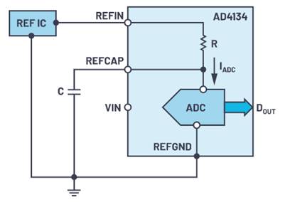
Figure 9. On-chip reference noise filter resistors simplify reference front-end design for CTSD ADCs
In the new front-end design, the reference IC is connected to the REFIN pin and the filter capacitor is connected to the REFCAP pin to form a noise filter for the noise of the reference IC. Since the value of on-chip resistor R and IADC are both functions of the same resistor material, there is no temperature drift (VREFADC) on REFCAP. The AD4134 also digitally self-calibrates the voltage drop across the on-chip resistors using a patented on-chip reference correction algorithm. Therefore, the reference driver design is simplified, and only the reference IC and capacitor values need to be selected according to the performance requirements.
The ADR444 is one of the low noise voltage reference ICs that can be used as a companion to CTSD ADCs. The AD4134 data sheet provides further details on capacitor value selection and internal/external digital gain calibration.
in conclusion
CTSD ADCS remove many barriers to achieving optimal precision performance and simplify front-end design. In the next article, we will describe how to process the output of the CTSD ADC modulator core into a final digital output format for use by an external digital controller for optimal processing. From the Sigma-Delta basics covered in this series of articles, the modulator output cannot be processed directly because it is sampled at a much higher rate. The sampling rate needs to be reduced to the output data rate (ODR) required by the application. Next, we’ll introduce a novel asynchronous sample rate conversion (ASRC) technique that allows the signal chain designer to tune the final ADC output to whatever ODR is desired, the ancient limitation of ODR being only a few times the sampling frequency no longer exists. Stay tuned for these interesting insights!
Reference circuit
“Driving Precision Converters: Choosing a Voltage Reference and Amplifier.” Analog Devices.
Mahaffey, Anna. “Driving a SAR ADC (Part 1): An Analog Input Model.” Analog Devices.
Shah, Anshul. “Why is Voltage Reference Noise Important?” Analog Dialogue, Volume 54, Number 1, March 2020.
author

Abhilasha Kawle
Abhilasha Kawle is Analog Design Manager, Linear and Precision Technologies, Analog Devices, Inc., Bangalore, India. She graduated in 2007 from the Indian Institute of Science, Bangalore with a master’s degree in Electronic Design and Technology.

Roberto Maurino
Roberto Maurino is a design engineer in the Precision ADC Division of Analog Devices in Newbury, UK. He received his Ph.D. from Imperial College London in 2005, and an engineering degree from the Politecnico di Torino in Italy and the Ecole Nationale Polytechnique in Grenoble in France in 1996.
The Links: FS35R12KT3 ADV7612BSWZ