

Content last revised on October 18, 2026
Benchtop Waveform Tuning: Mitigating Stress via Reinforced Insulation Barrier Integrity on FS35R12KT3
Separate a genuine gate disturbance from a measurement artifact by checking probe placement, common-mode capability, and the connection between the probe reference and the emitter terminal. As a Design Consideration, long measurement loops can collect switching noise and exaggerate apparent gate ringing. Capture the driver output and the gate waveform together where instrumentation permits; a disturbance appearing only at the module terminals directs attention toward the interconnect, shared emitter impedance, and local coupling.
The isolation barrier belongs to the complete gate-drive assembly, including its signal isolator, isolated supply, circuit board spacing, and connectors. Reinforced insulation classification and common-mode transient immunity are separate properties requiring their own component documentation and applicable equipment assessment. Neither property follows from the FS35R12KT3’s collector-emitter voltage rating. Treat isolation coordination as a system requirement rather than attributing an unsupported barrier withstand rating or transient-immunity value to this module.
For insulation coordination, an Engineering Recommendation is to review clearance and creepage against the actual working voltage, installation environment, insulating materials, and equipment standard. Inspect the assembled board for contamination, misplaced hardware, and conductive residue that could compromise the intended separation. An insulation test requires an approved procedure appropriate to the connected electronics; its voltage and duration should come from the relevant assembly documentation and test standard.
Gate-loop layout deserves attention before resistance changes. As a Design Consideration, place the outgoing gate conductor and its emitter return close together, keep the driver connection compact, and avoid routing this loop alongside switching power conductors. Shared emitter impedance can move the driver’s apparent reference during current transitions. The resulting gate waveform can resemble inadequate drive even when the driver supply remains stable.
Miller coupling can also raise the gate voltage of an inactive switch while the opposing device changes collector voltage. An Engineering Recommendation is to examine the inactive gate during the actual commutation event, including its off-state holding behavior and any supported clamp function. Select damping and gate-control measures from the driver’s capabilities and measured response. Increasing resistance without checking both transitions can reduce ringing while increasing switching loss or delaying turn-off.
Infineon’s IGBT Modules Overview provides manufacturer context for distinguishing module families during component evaluation. Technology-specific information also needs careful separation: the discussion of Infineon TRENCHSTOP™ IGBT7 concerns a different technology context and does not establish FS35R12KT3 switching, packaging, or reliability specifications.
FS35R12KT3 Circuit Protection & Reliability: Calibrating Thermal Cycling Margins in Braking Applications
Trace the braking-current path on the equipment schematic before assessing deceleration stress: identify the DC-link connection, braking switch, resistor assembly, and control feedback. Do not assign an internal braking transistor to the FS35R12KT3 without an established circuit diagram. The braking stage must be identified from the equipment architecture, because regenerated energy reaches the DC link through the motor inverter while its eventual absorption depends on the installed braking or regeneration arrangement.
As a Design Consideration, braking evaluation should account for load inertia, deceleration profile, repetition rate, initial resistor temperature, and the controller’s response to rising bus voltage. Check the resistor’s pulse-energy and average-power limits separately. A resistor that tolerates an individual stop can still accumulate excessive heat during repeated operation. The braking switch also needs assessment for its actual pulse current, switching loss, and heat-removal path.
Thermal cycling assessment should follow the measured operating sequence. An Engineering Recommendation is to correlate current and switching activity with temperature measurements at accessible, documented locations, then use the applicable thermal model to assess junction conditions. Examine mounting contact, interface condition, and cooling performance when temperatures drift between otherwise comparable runs. An external temperature reading alone does not establish the semiconductor junction’s peak temperature or cycling amplitude.
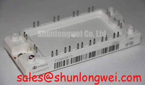
For replacement evaluation, place the FS35R12KT3 beside the linked BSM75GP120 as a comparison candidate rather than assuming equivalent circuitry. The table separates the supplied FS35R12KT3 specifications from information that requires the corresponding manufacturer datasheet. This preserves a useful purchasing comparison without turning a related product link into a substitution approval.
| Selection item | FS35R12KT3 | BSM75GP120 |
|---|---|---|
| Manufacturer | Infineon | Consult Datasheet |
| Rated voltage | 1200 V — Official Specification | Consult Datasheet |
| Rated current | 35 A — Official Specification | Consult Datasheet |
| Package category | Module — Official Specification | Consult Datasheet |
| Internal circuit, terminal arrangement, and dimensions | Consult Datasheet | Consult Datasheet |
| Driver and cooling compatibility | Equipment-specific assessment | Equipment-specific assessment |
Desaturation protection requires a timing review of the entire detection chain. As a Design Consideration, the monitored collector-emitter voltage is interpreted alongside gate state, turn-on blanking, sensing-network behavior, propagation delay, and the driver’s shutdown response. Normal turn-on transients must be distinguished from a fault without extending exposure beyond the device’s documented short-circuit capability. A universal detection-time prescription would bypass these dependencies.
Where the driver supports staged shutdown, an Engineering Recommendation is to evaluate its controlled initial turn-off and subsequent gate discharge against the fault current and resulting collector-voltage excursion. Slower shutdown can reduce inductive overshoot while increasing fault energy. Protection timing therefore belongs to a coordinated review of the module’s applicable limits, driver behavior, DC-link conditions, and measured fault response.
Semiconductor fuse coordination addresses another part of the fault path. As a Design Consideration, compare the fuse manufacturer’s pre-arcing and total-clearing I²t information with the protected circuit’s documented withstand limits under the relevant voltage and prospective current. Check interrupting capacity and clearing behavior as well. Fuse coordination alone does not establish package containment or guarantee that a semiconductor survives a hard short circuit.
Related power stages require separate driver and supply assessment. The BSM100GB120DLC can be reviewed as another module within a broader system comparison, with its actual circuit role established from its own documentation. Thyristor trigger-current, trigger-voltage, and pulse-train criteria concern thyristor stages; they are not substitutes for evaluating an IGBT’s gate-voltage waveform and driver current capability.
Field Diagnostics & Commissioning: Mitigating Commutation Turn-Off Voltage Spikes in FS35R12KT3 Topologies
Align the collector-voltage capture with the commutating current waveform to distinguish turn-off overshoot from the disturbance produced during diode recovery. As a Design Consideration, current commutation through the freewheeling path can produce recovery current and excite parasitic inductance and capacitance. The observed response depends on current, temperature, bus voltage, and gate-drive conditions, so compare captures taken under controlled and recorded operating conditions.
Measure recovery behavior through a suitable current-sensing arrangement, accounting for bandwidth, insertion effects, and timing alignment with the voltage probe. An Engineering Recommendation is to examine peak reverse current, the recovery-current slope, and subsequent ringing together. A sharp current transition can contribute to voltage disturbance, but waveform shape alone does not identify a defective diode or prove a particular recovery classification.
Power-loop inspection should follow the physical commutation path through the DC-link connection, switching devices, and return conductor. As a Design Consideration, connection geometry and joint condition influence the effective loop inductance. Check disturbed busbar joints and capacitor connections before attributing a changed waveform entirely to the replacement module. Unequal routing can also create unequal transient conditions between otherwise similar switching positions.
Engineering Recommendation: Keep paired power paths compact and geometrically balanced to reduce commutation-loop inductance, then verify turn-off voltage margin with an appropriately controlled double-pulse test.
Gate resistance and snubber selection should follow the measured source of oscillation. As a Design Consideration, turn-on resistance affects the opposing diode’s commutation rate, while turn-off behavior affects the switched device’s voltage excursion. An RC snubber introduces damping but also dissipates energy and changes current paths. Evaluate component pulse capability, temperature rise, and waveform response before accepting a revised network.
For application compatibility, a precision stepper or BLDC motor servo motion actuator is a possible evaluation context, subject to its actual inverter topology, current demand, switching frequency, control strategy, and cooling arrangement. The 1200 V, 35 A ratings support the initial component-class comparison; the terminal map, mounting interface, gate-drive behavior, and operating limits determine whether the FS35R12KT3 fits that particular assembly.
The discussion of Resonant Topologies in Home Appliances offers a separate reference for understanding how circuit topology changes commutation conditions. Apply its topology distinctions only where relevant to the circuit under examination. For the installed FS35R12KT3 assembly, retain the measured gate, collector-voltage, and current traces with the operating conditions so that future troubleshooting can identify a changed connection, driver response, or cooling condition against a meaningful commissioning baseline.