

Content last revised on September 14, 2026
BSM100GB120DLC Operational Boundaries: Evaluating Thermal Interface Material Thickness Limits
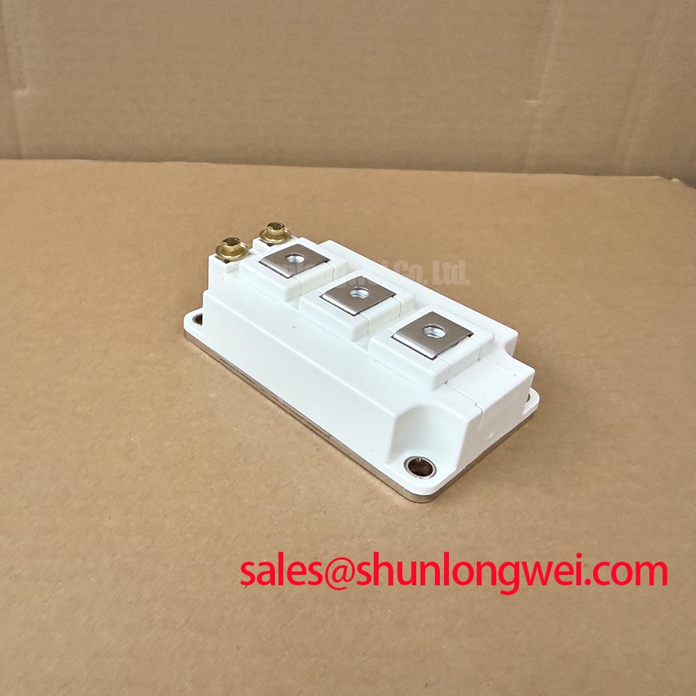
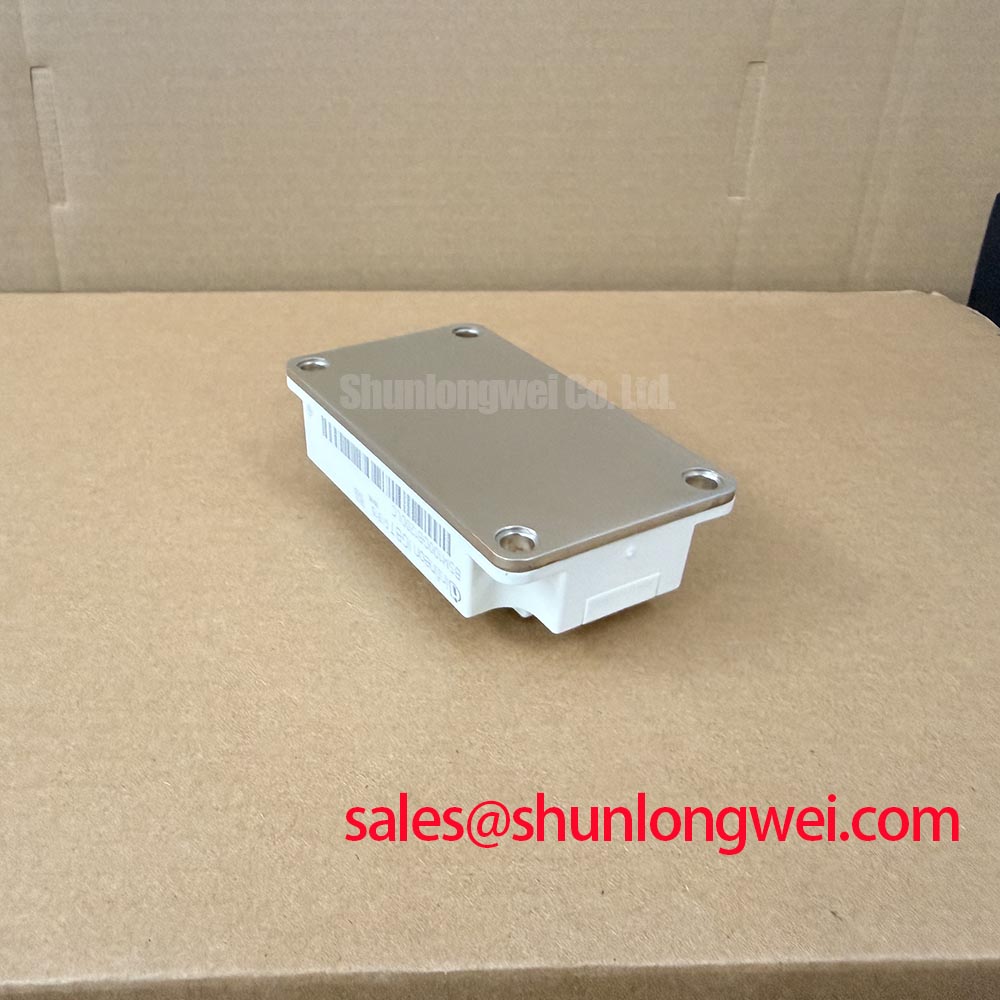
The thermal path between the module baseplate and heatsink should be treated as part of the power circuit’s reliability work. A clean heatsink surface, even mounting pressure, and a controlled thermal interface material layer help reduce contact resistance. The stated TIM thickness range in the supplied engineering brief is a Design Consideration, not an official electrical rating for this specific module. The final application should follow the TIM manufacturer’s process window and the module supplier’s mechanical instructions.
Apply only enough thermal compound to fill surface irregularities after the two mating surfaces have been cleaned with a suitable process. Excess compound can increase the thermal path and contaminate nearby insulation surfaces, while insufficient coverage can leave air pockets beneath the baseplate. A practical production check is to inspect the compound transfer pattern after a controlled trial assembly. An incomplete imprint should prompt a review of heatsink flatness, surface cleanliness, mounting pressure, and the selected interface material.
Baseplate curvature compensation must be handled by the mounting method rather than by excessive torque. Place the module on the heatsink without forcing one corner down, align all mounting points, and tighten fasteners progressively in a diagonal or manufacturer-specified sequence. The exact torque is a manufacturer and hardware dependent value. If the original equipment documentation is unavailable, the maintenance team should not substitute a guessed torque figure; verify the fastener size, washer arrangement, thread condition, and module mounting drawing first.
Leave practical clearance around the power terminals and gate control area so that busbars, driver wiring, and insulation barriers do not press against the housing during vibration or thermal cycling. Clearance must also allow a probe or inspection tool to reach the terminals without disturbing the assembly. Designers should verify creepage and clearance against the working voltage, pollution environment, insulation system, and applicable equipment standard rather than copying a generic spacing value.
Thermal commissioning should combine heatsink temperature, module case temperature, current waveform, and the equipment’s thermal protection response. The transient thermal impedance network, commonly represented through the module’s Zth data, converts a switching loss pulse into a junction temperature rise. That calculation must use the actual pulse duration, duty cycle, case temperature, cooling conditions, and manufacturer-published thermal curves. A short current pulse should not be assessed with a steady-state thermal resistance alone.
⚠️ Maintenance Note: Schedule periodic heatsink cleaning and monitor the module-to-heatsink temperature rise, especially where blocked airflow or moisture condensation can develop.
Transient Dynamics & Electrical Design: High-Frequency Commutation Loop Inductance on BSM100GB120DLC
During commissioning, verify the terminal identity from the original Infineon documentation and compare every power and control connection with the inverter schematic before applying the DC link. Do not infer an auxiliary emitter, gate, or sensing terminal from physical position alone. If a control terminal is provided in the applicable drawing, route its return separately from high-current emitter paths as required by the gate-driver design, and confirm the reference point with continuity checks while the system is fully isolated.
Commutation loop inductance influences the voltage overshoot produced during rapid current change. The relationship can be considered in the form Vpeak = VDC + Lσ × (di/dt), with the actual peak determined by the complete switching network, measurement bandwidth, device behavior, and clamp arrangement. This is an Engineering Calculation used to frame the design review, not a guaranteed switching limit for the BSM100GB120DLC.
Use a compact, symmetrical planar busbar arrangement where the topology permits it. Keep the forward and return paths close together, reduce unnecessary conductor area, and avoid routing the gate-driver loop alongside the highest-current commutation path. The engineering brief identifies a low-inductance target for evaluation, but that target is a system design objective rather than an official module parameter. Confirm the result with a suitable high-bandwidth measurement method and verify the peak voltage against the actual DC-link operating condition.
Snubber selection should begin with measured ringing, switching energy, capacitor voltage stress, pulse repetition, and resistor heating. A larger capacitor is not automatically safer because it can increase turn-on or turn-off loss and alter the gate-driver burden. Designers should select and validate the snubber as part of the complete inverter network, then check the module’s junction temperature using the published transient thermal data.
Busbar fastening requires mechanical control as well as electrical continuity. Inspect contact surfaces for oxidation, confirm that washers and supports cannot loosen under vibration, and use the equipment manufacturer’s approved locking method. After reassembly, measure the voltage drop across the intended current path during a controlled test and compare phase legs under matching load conditions. An abnormal difference may indicate contact resistance, asymmetrical geometry, probe error, or a control mismatch; it should be isolated through comparative measurements rather than assigned to the module immediately.
For broader device context, engineers can review the Infineon IGBT Modules & Discretes Official Portfolio and the Infineon IGBT Modules Overview. These references help place the component within the manufacturer’s wider power semiconductor range without replacing the specific documentation required for this part number.
Assembly Integrity & Layout Architecture: Implementing Fault-Clearing Dynamics for BSM100GB120DLC
Short-circuit protection must be reviewed at the system level before a replacement module is energized. A desaturation circuit, current sensor, or other approved detection method should be matched to the gate-driver architecture, noise environment, blanking behavior, and fault energy. The requested Type-I and Type-II protection timing is an application objective from the engineering brief, not an official published rating supplied here. Designers should verify the actual detection and turn-off delay with a controlled test fixture and the final driver hardware.
Two-stage soft turn-off is commonly evaluated when a hard gate discharge could produce excessive inductive voltage. The first action limits the fault current transition, while the subsequent action completes turn-off under conditions set by the driver and power loop. The correct sequence depends on gate resistance, driver output capability, parasitic inductance, clamp behavior, DC-link voltage, and short-circuit test conditions. Do not transfer a protection delay or gate voltage from another module without checking the relevant datasheet and driver application notes.
Place the fault-detection return path so that power-emitter voltage movement does not corrupt the control reference. Where the module drawing identifies a separate auxiliary emitter or driver return, keep that conductor distinct from the high-current emitter connection until the intended reference point. The physical routing should be short, mechanically supported, and protected from capacitive coupling to the switching node. If the applicable drawing does not confirm a Kelvin connection, the system integrator should verify the terminal definition before changing the harness.
Fault testing should begin with reduced stored energy and an instrumented setup capable of capturing gate voltage, collector-emitter voltage, current, and driver fault response. Check that the driver enters its fault state, that the DC-link discharge path operates as intended, and that repeated testing does not exceed the module’s published safe operating conditions. A protection circuit that works on a bench may behave differently after cable installation, enclosure assembly, or busbar replacement, so the final layout must be tested in its installed configuration.
Reliability discussions should remain tied to measured electrical and thermal stress. The technical guide Unlocking Efficiency in Industrial Drives provides additional application context for industrial IGBT technology. It should be read alongside the specific BSM100GB120DLC documentation rather than treated as a substitute for its official ratings or switching data.
Field Diagnostics & Commissioning: Derating Guidelines and Mismatched Parameters in BSM100GB120DLC Topologies
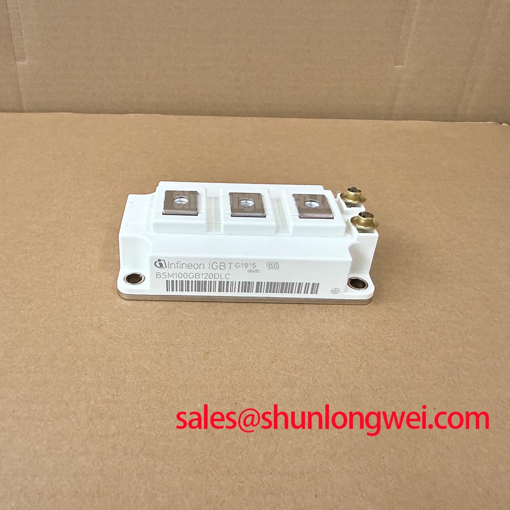
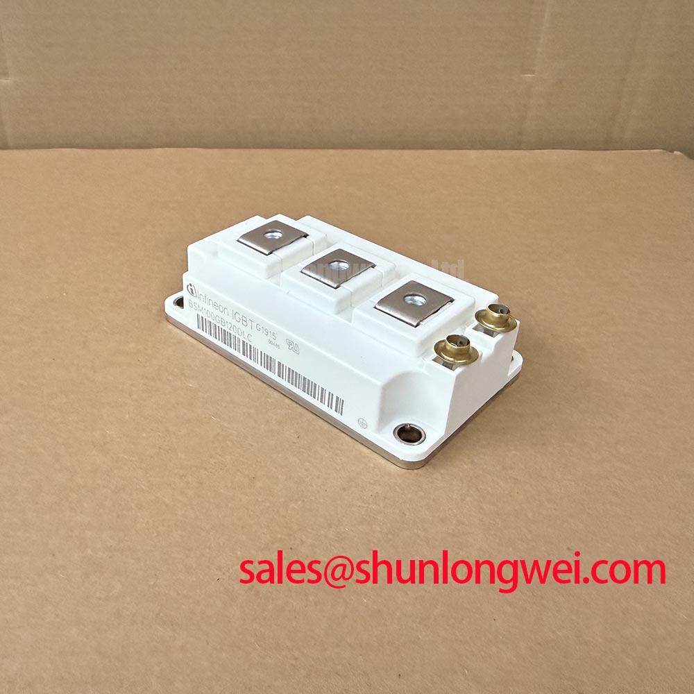
When replacing a module in a commercial string inverter or microgrid energy-storage converter, compare the complete topology before installation. Confirm the DC-link voltage, phase-leg arrangement, gate-driver supply requirements, protection thresholds, cooling path, busbar geometry, and control firmware assumptions. The official values supplied for this product are 1200.0 V rated voltage and 100.0 A rated current; actual allowable current depends on temperature, switching conditions, duty cycle, cooling, and the manufacturer’s detailed curves.
Current sharing in parallel IGBT arrangements requires both static and dynamic evaluation. The positive temperature coefficient often associated with on-state voltage can support static current balancing, but it does not remove the need for matched electrical paths. Gate-loop length, common-emitter impedance, driver timing, busbar inductance, and thermal coupling can produce unequal transient current. Designers should use symmetrical gate wiring, measure each branch during switching, and confirm that the hottest branch remains within the applicable transient and steady-state thermal limits.
A field replacement inspection should compare the removed unit and replacement position without assuming that similar appearance means identical behavior. Record terminal markings, connector orientation, heatsink contact condition, gate resistor arrangement, snubber placement, and phase-leg wiring. A mismatched parameter may appear as unequal switching voltage, unusual ringing, abnormal gate waveform, or a phase-specific temperature rise. Each symptom requires comparison with a known-good leg and an oscilloscope measurement at the correct reference point.
For the rectifier or complementary stage of an energy-conversion system, engineers may also evaluate the related BSM75GD120DLC where the circuit documentation identifies a compatible role. This is a neutral topology reference, not a prescriptive substitute for the specified design. Any cross-reference must be checked for voltage class, current conditions, package geometry, terminal assignment, thermal behavior, gate-drive requirements, and protection coordination.
The FS100R12N2T4 may be reviewed as a comparison device during hardware evaluation, but the final decision belongs to the system engineer after electrical, mechanical, thermal, and protection compatibility checks. Confirm the original equipment bill of materials and application documentation before changing the approved part number.
During first power-up, use a controlled DC-link ramp, verify gate signals on every switching position, and check phase symmetry under a limited-load condition before normal operation. Inspect the enclosure for airflow restriction, condensation risk, and contamination paths. Where the inverter operates near its thermal boundary, use measured case temperature and calculated pulse junction temperature rather than relying on heatsink temperature alone. Any derating curve, lifetime estimate, insulation claim, EMC result, or safety certification must come from the applicable manufacturer documentation or equipment-level test record.