


Content last revised on September 30, 2026
Assembly Integrity and Layout Architecture for Fault Clearing
| Manufacturer | Infineon |
|---|---|
| Part Number | FS10R06VE3_B2 |
| Product Category | IGBT Module |
| Rated Voltage | 600 V |
| Rated Current | 10 A |
| Package | Module |
Measure the power terminals and gate control path with the equipment isolated, then compare the cold impedance pattern with a known good assembly before applying a replacement FS10R06VE3_B2. A short reading between the main terminals, an unexpected gate to emitter path, or a visibly damaged housing requires circuit isolation before any powered test.
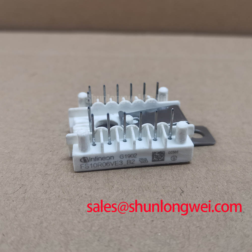
The FS10R06VE3_B2 is an Infineon IGBT module with an official rated voltage of 600 V, an official rated current of 10 A, and a module package. These figures define the component identification boundary. They do not by themselves define the safe DC bus, switching frequency, short circuit duration, junction temperature, or allowable overload for a complete inverter. Those values must be established from the applicable device documentation and the system operating envelope.
For a compact industrial inverter or high speed CNC spindle drive, fault clearing should be examined as a coordinated function rather than as a gate driver feature alone. A desaturation detector monitors the collector emitter condition after the IGBT is commanded on. A Type I response may provide the initial fault recognition and controlled gate action, while a Type II sequence can provide a softer turn off after the fault is confirmed. The exact timing, blanking interval, soft turn off current, and short circuit safe operating area must be verified against the selected gate driver and the official switching data.
Design Consideration: the frequently discussed sub ten microsecond short circuit response is a system target that cannot be assigned to this module without a matched driver, layout, current path, and validated short circuit data. If the protection chain is being evaluated around that target, use a differential probe and current probe to capture the fault command, gate voltage, collector emitter voltage, and collector current on the same time base. Confirm that the turn off transient remains within the voltage boundary during the actual DC bus test.
Keep the high current commutation loop physically compact and separate the gate return from the power return. Minimize stray inductance to reduce turn off overshoot, but allow the final geometry to be determined by the module terminals, bus structure, insulation system, and measured switching waveform. Clearance and creepage must be checked against the equipment working voltage, pollution environment, insulation material, and applicable safety standard rather than copied from a generic layout rule.
When the gate driver requires galvanic isolation, the Infineon EiceDRIVER™ Galvanic Isolated Gate Driver ICs provide a relevant reference family for evaluating isolation, desaturation handling, interlock behavior, and gate power architecture. The selected driver remains a system choice, and its output current, protection delay, and supply arrangement must be matched to the actual module circuit.
A failed module should be removed only after checking the gate resistor, driver supply, desaturation diode network, clamp components, and current sensor path. If the replacement repeatedly fails at startup, capture the gate waveform at the module terminals instead of measuring only at the driver output. A difference between those two locations can expose common impedance, connector resistance, or ground bounce in the control path.
Thermal Electrical Optimization for Regenerative DC Bus Surges
Probe the DC link during controlled motor deceleration and record the peak voltage, duration, repetition rate, and braking command before selecting a braking path around the FS10R06VE3_B2. A high bus rise can involve regenerative energy, braking control timing, capacitor condition, wiring inductance, or an incorrectly coordinated clamp, so the waveform should be reviewed with the drive operating under its normal mechanical load.
In a spindle drive, the braking circuit converts motor kinetic energy into heat or transfers it through an energy recovery path. The braking IGBT, ballast resistor, control threshold, and DC link capacitor must be evaluated as one energy system. The resistor is selected from the required pulse energy, duty cycle, thermal recovery, and permissible bus voltage. The braking semiconductor is then checked for voltage stress, current stress, switching loss, and thermal impedance. The 600 V rating of this module is an official component parameter, not an automatic permission to operate a DC bus at that level.
Designers should also review the negative and positive bus conductors between the capacitor, braking switch, and power module. A long or asymmetrical path can add inductive voltage during the braking transition. Minimize the high current loop and verify the resulting peak with a properly rated differential probe. The acceptable margin is determined by the equipment DC bus, transient conditions, insulation coordination, and the device switching data.
High speed semiconductor fuse coordination requires more than comparing nominal current ratings. The fuse clearing characteristic, let through energy, device short circuit capability, bus capacitance, and wiring impedance all influence the fault event. Compare the fuse I²t curve with the relevant surge and short circuit limits supplied for the complete semiconductor assembly. If those data are unavailable, treat the fuse as a separate protective layer and do not infer that it will prevent module damage in every fault sequence.
For a front end and inverter topology, the rectifier or active front end may be reviewed alongside a related power stage such as FF300R12KE4_B2. This is a neutral topology reference rather than a direct replacement recommendation. Voltage class, current capability, gate drive requirements, package interfaces, thermal path, and protection behavior must be checked independently for each position in the circuit.
Inspect the module mounting surface for contamination, uneven contact, and mechanical distortion. Thermal interface material should be applied as a uniform thin layer suitable for the heatsink and module interface. Field Alert: disconnect the DC link and verify the stored energy has fallen to a safe measured condition before touching the module terminals or removing a gate cable.
During commissioning, use a staged bus ramp or current limited test method selected by the system engineer. Observe the DC bus at idle, during acceleration, during deceleration, and during repeated braking cycles. A single successful stop does not establish resistor pulse endurance or thermal stability.
Benchtop Waveform Tuning and Transient Thermal Impedance
Capture the collector emitter voltage, gate emitter voltage, phase current, and heatsink temperature during a representative switching pulse, then correlate the waveform with the load current and pulse repetition pattern. This is the fastest way to separate a gate loop problem from a thermal accumulation problem in the FS10R06VE3_B2 evaluation.
Transient thermal impedance describes how the junction to case thermal path responds to a pulse over time. The case temperature alone can look acceptable while the semiconductor junction experiences a much higher short duration temperature rise. A multi RC thermal model can estimate that response when its coefficients come from the relevant manufacturer data. The peak junction temperature is then checked against the specified operating boundary using the measured or calculated power pulse. Do not substitute a generic thermal curve for the official curve of the device under evaluation.
Measure the module case temperature at a repeatable location and record heatsink temperature separately. The thermal interface, mounting pressure, heatsink flatness, airflow, and sensor attachment method affect the result. When the waveform shows rising conduction voltage or increasing turn off loss over repeated pulses, compare the electrical loss trend with the thermal trend rather than assigning the symptom to one component immediately.
Gate tuning should begin with the driver manufacturer’s permitted output conditions and the module switching data. Adjustments to gate resistance, turn on speed, turn off speed, and active clamp behavior should be made one variable at a time. Watch for the tradeoff between lower switching loss, higher electromagnetic emission, overshoot, and cross conduction. The final setting is system determined and should be validated at the highest intended bus voltage, current, and temperature.
Freewheel diode reverse recovery can affect both the IGBT turn on waveform and radiated EMI. The reverse recovery softness factor, commutation loop inductance, diode current, and gate control interact during the transition. Review the diode waveform with a short probe connection and compare the ringing frequency and amplitude before changing the gate network. A softer recovery profile can reduce some voltage disturbance, but the actual effect depends on the complete bridge and load arrangement.
Bootstrap gate supplies need adequate high frequency charge replenishment for the selected duty cycle and gate charge. Check the bootstrap capacitor voltage directly at the driver pins during the fastest switching sequence, including dead time and repeated high duty operation. Diode recovery, supply impedance, capacitor placement, and common mode displacement can reduce the available gate drive even when the static supply measurement appears normal. The required capacitance and recharge strategy must be calculated from the chosen driver and switching conditions.
For broader high voltage switching comparisons, engineers may consult The 1200 V CoolSiC™ MOSFET Advantage in Three. That material can support topology and switching discussions, but it does not change the official voltage or current identity of the FS10R06VE3_B2.
Field Diagnostics for Miller Coupling and Gate Voltage Spikes
Place the oscilloscope reference at the module gate emitter return and inspect the off state while the opposite switch commutates; measure the actual gate voltage at the module pins, not only at the driver board. A positive gate spike, irregular dead time, or unequal phase behavior may indicate capacitive coupling, common emitter inductance, driver return movement, or an unstable isolated supply.
Gate-collector capacitance and high dv/dt can transfer current into an off state gate circuit. An active Miller clamp provides a low impedance path during the off interval when the selected driver supports that function. Its effectiveness depends on the driver placement, gate loop inductance, clamp threshold, emitter reference, and switching transition. Review these conditions with the driver documentation and confirm the clamp waveform under the highest practical switching stress.
Negative gate bias is sometimes used as a design option to increase off state immunity, but a range such as minus five to minus fifteen volts must not be applied to this module as a universal prescription. The permitted gate emitter voltage, driver supply arrangement, insulation system, and transient behavior must come from the applicable device and driver documentation. Verify the negative level at the module terminals and check for overshoot during both turn on and turn off.
Separate the auxiliary emitter or Kelvin return, where the selected module and driver interface provide one, from the high current emitter path. Route the control return directly to the driver reference and avoid sharing copper with the commutation current. This reduces common mode ground bounce, but the final routing must follow the actual terminal arrangement of the package rather than an assumed pin definition.
When a bootstrap supply is used, monitor its charging diode and capacitor during the complete PWM pattern. High frequency charge loss, diode recovery current, or insufficient refresh time can make the gate spike appear intermittent. An isolated gate supply can remove some bootstrap limitations, while introducing its own common mode and isolation design requirements.
Thyristor gate triggering belongs to a different control problem than IGBT gate drive. If a spindle inverter includes a thyristor input stage, verify its gate trigger current, gate trigger voltage, pulse width, and pulse train behavior from the thyristor data. Strong pulse trains can improve trigger consistency under electrical noise, but they must be coordinated with the firing circuit, isolation, thermal duty, and device limits. Do not use thyristor trigger values to configure the IGBT gate terminal.
For final commissioning, compare each phase at identical bus voltage and load conditions. Check gate amplitude, turn off behavior, dead time, collector emitter overshoot, current sharing, and temperature rise. Any unexplained difference should be isolated by testing the driver, module, load, and wiring separately rather than treating one waveform as proof of a single failure mechanism.