

Content last revised on October 9, 2026
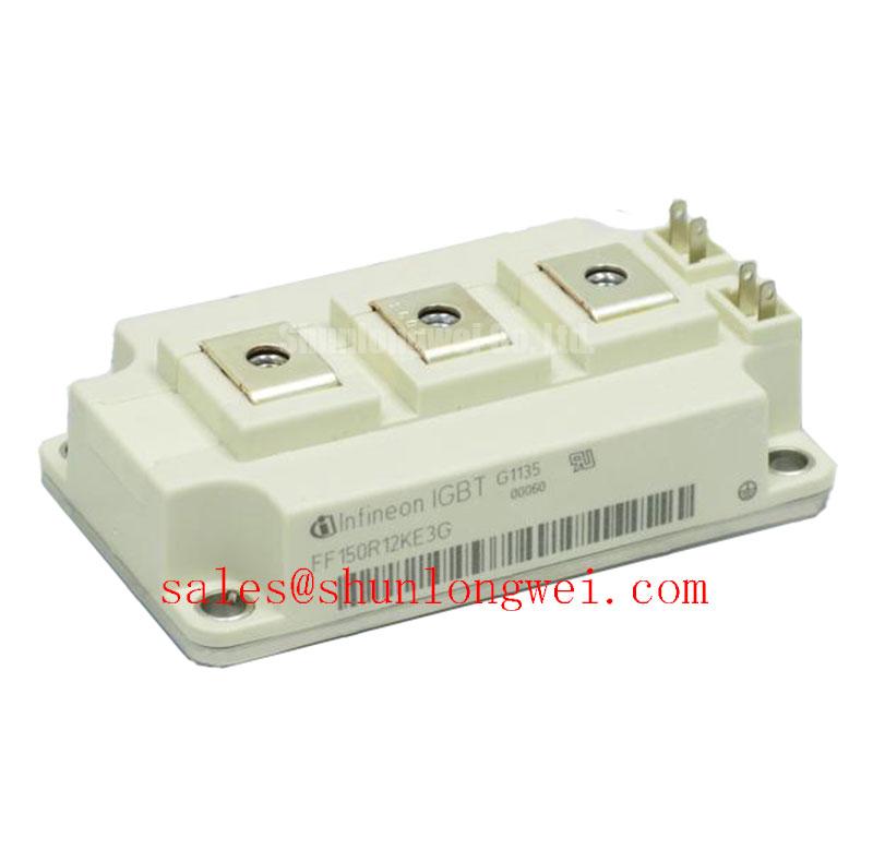
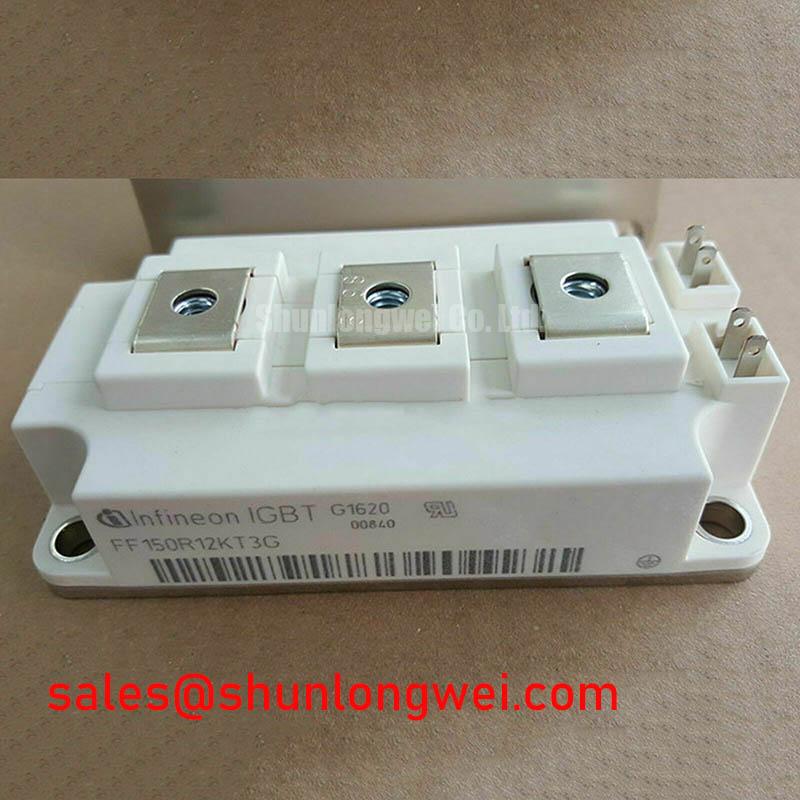
FF150R12KT3G Infineon 1200V 150A IGBT Module
Begin a bench evaluation by confirming the nameplate identity, checking the module housing for mechanical damage, and verifying the intended DC bus boundary before applying any gate signal. The Infineon FF150R12KT3G is an IGBT module with an official rated voltage of 1200.0 V, an official rated current of 150.0 A, and a module package. These are manufacturer-level product parameters supplied for identification and engineering selection; switching, thermal, gate-drive, diode, and isolation limits must be confirmed from the applicable Infineon documentation before final design release.
| Manufacturer | Infineon |
| Part number | FF150R12KT3G |
| Rated voltage | 1200.0 V |
| Rated current | 150.0 A |
| Package | Module |
Thermal Time Constants and Peak Junction Temperature Margin Calculation
For a commercial string inverter or microgrid storage converter, evaluate the module during the actual overload pulse rather than relying only on steady-state heatsink temperature. A transient thermal network represents junction-to-case behavior through multiple RC sections, allowing the engineering team to estimate how a short current pulse contributes to peak junction temperature. The calculation should use the verified switching loss, conduction loss, case temperature, pulse duration, and the manufacturer’s thermal impedance data for the exact device revision.
The relevant design margin is system-dependent. Engineers should compare the calculated peak junction temperature with the official maximum junction temperature, then validate the result with thermocouples or other suitable measurement methods during controlled power testing. Switching frequency, coolant or airflow conditions, heatsink flatness, thermal interface quality, and overload repetition all affect the result. A higher current pulse does not automatically produce the same thermal response as continuous operation, because the effective impedance changes with pulse width.
When field equipment trips under high solar input, inspect the complete thermal path before attributing the event to semiconductor failure. Check mounting contact, heatsink temperature distribution, fan or coolant performance, current-sensor scaling, and the recorded switching waveform. The Field Engineer’s Handbook provides a useful reference framework for structured testing and failure analysis.
FIT Rates in High-Altitude Solar and Wind Farms
FIT and Single Event Burnout analysis require authoritative reliability data, application conditions, and a defined mission profile. This product page does not assign a numerical FIT rate, SEB probability, or operating lifetime to the FF150R12KT3G. At elevations above 2000 m, reduced air density can affect cooling and external insulation coordination, while terrestrial neutron exposure may become a consideration for high-voltage power semiconductors. These effects should be reviewed with the manufacturer’s reliability documentation and the system safety assessment rather than estimated from altitude alone.
For a high-altitude solar inverter, the design team should verify DC-link voltage headroom against switching overshoot, temperature rise, cooling airflow, and the selected switching frequency. A converter operating anywhere across a broad frequency range requires loss measurements at the real gate resistance, current profile, modulation pattern, and ambient condition. The same approach applies to wind-farm converters, where enclosure ventilation, filter loading, and altitude-related cooling changes can shift the thermal operating point.
Short-circuit coordination also needs measured evidence. The I²t capability of a semiconductor fuse, the converter’s detection delay, gate turn-off behavior, and the module’s specified short-circuit withstand conditions must be checked together. Engineers should not infer a safe clearing time from the 1200 V or 150 A nameplate values alone.
Negative Gate Bias and Active Miller Clamping in Fast-Switching Half-Bridges
In a half-bridge, collector-to-emitter voltage transition can couple through the Miller capacitance and disturb the opposite device gate. The practical objective is to keep the gate loop low impedance, minimize common-emitter inductance, and separate power-current paths from gate-return paths. Negative gate bias may be evaluated where the approved driver, insulation system, and gate-emitter limits support it, but the FF150R12KT3G product data supplied here does not establish a universal negative-bias setting.
Active Miller clamping can provide a controlled low-impedance path during the off-state transition. Its effectiveness depends on driver placement, clamp timing, gate-loop inductance, the external gate network, and the measured dv/dt of the complete inverter. Designers should verify gate-emitter voltage directly at the module terminals with suitable probing techniques. A false clean waveform at the driver board does not prove that the semiconductor gate sees the same voltage.
💡 Pro Tip: Keep the gate-drive loop physically compact and validate the Kelvin return path, because a long shared emitter connection can convert switching-current inductance into apparent gate-voltage error and cross-conduction risk.
For parallel-device studies or current-sharing analysis, consult Infineon’s IGBT paralleling application note. It should be read alongside the exact FF150R12KT3G datasheet and the inverter’s measured commutation behavior.
Baseplate Convexity Compensation and Screw Tightening Sequence
Thermal installation begins with a clean heatsink surface, correct interface material selection, and a mechanical check of the baseplate and mounting plane. The interface layer should be thin and continuous, with voids, contamination, and excessive compound avoided. Any proposed thickness range is a general design consideration, not an official FF150R12KT3G specification, unless confirmed by the applicable mounting instruction.
Baseplate convexity should be assessed against the heatsink surface and the manufacturer’s permitted mounting conditions. Tighten fasteners progressively in a diagonal or crosswise sequence so the module seats evenly. The final torque, screw type, washer arrangement, and sequence must follow the relevant Infineon mechanical data; do not transfer a torque value from another module family.
After installation, inspect the contact pattern where practical and measure thermal behavior under controlled load. Uneven temperature distribution, repeated thermal alarms, or abnormal case movement should prompt a review of mounting pressure, heatsink flatness, interface material coverage, and enclosure vibration. In a rectifier and inverter system, the related FZ600R12KE4 may be evaluated as a complementary front-end device, while the technically related FF150R12ME3G can be reviewed separately for application compatibility rather than treated as an automatic substitute.