


Content last revised on September 29, 2026
Benchtop Waveform Tuning: Mitigating Stress via Baseplate Convexity Compensation and Screw Mounting
| Parameter | Official Specification |
|---|---|
| Manufacturer | Infineon |
| Part number | BSM150GB170DLC |
| Product category | IGBT Module |
| Rated voltage | 1700.0 V |
| Rated current | 150.0 A under the specified datasheet conditions |
| Package | Module |
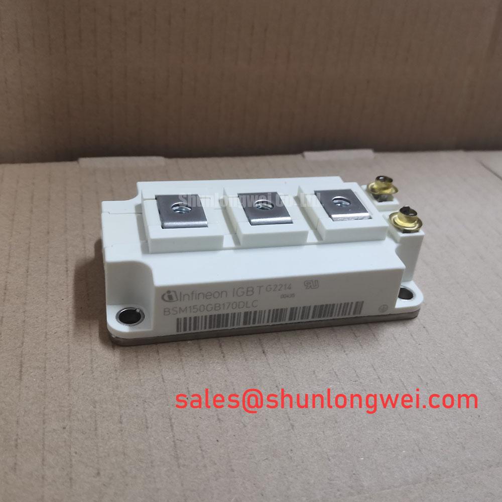
Measure the switching waveform at the module terminals with a properly referenced differential probe, then inspect the mounting interface if the observed overshoot or ringing changes after mechanical service. The BSM150GB170DLC is specified as a 1700.0 V, 150.0 A Infineon IGBT module; these are official product specifications subject to the applicable datasheet conditions, not a substitute for the voltage and current limits of the complete converter.
As a Design Consideration, the thermal interface material should form a continuous, controlled film between the module baseplate and heatsink. Excess compound can increase thermal resistance, while insufficient coverage can leave local air gaps. A clean heatsink, even pressure distribution, and a surface free from burrs are more important than applying a visibly thick layer. The suggested 50 to 100 µm interface range is a general integration reference only and is not an Infineon specification for this part.
Check the baseplate for uneven contact by inspecting the removed interface material after a controlled trial fit. An uneven contact pattern can concentrate pressure in some areas and leave others poorly coupled. Compensation should be handled by the system mechanical design, using a suitable heatsink flatness process and a mounting sequence that distributes load progressively. Torque values must come from the original mechanical documentation or the validated assembly procedure rather than from the electrical rating.
For waveform work, keep the power commutation path compact and route the gate-drive return beside its corresponding gate path. Compare turn-on and turn-off traces at matched probe locations. If only one switching position shows excessive ringing, inspect loop symmetry, terminal pressure, busbar spacing, and probe-ground error before changing the gate resistor. The Infineon TRENCHSTOP™ IGBT7 technical discussion provides useful industry context on switching behaviour and module reliability, but it does not establish additional ratings for this model.
Field Diagnostics & Commissioning: Thermal Feedback in BSM150GB170DLC Topologies
Record collector-emitter voltage, phase current, heatsink temperature, and gate waveform together during commissioning; a thermal rise without a corresponding load change warrants inspection of interface condition, airflow, terminal pressure, and switching balance. The module’s 150.0 A rating applies under the specified datasheet conditions, while the usable current in a PCS depends on switching frequency, cooling, duty cycle, ambient conditions, and the complete thermal design.
A positive temperature coefficient of the on-state voltage is commonly considered when paralleling IGBT devices because it can support static current sharing as temperature changes. This is a Design Consideration, not a guarantee of dynamic current balance. Dynamic sharing remains strongly affected by gate-loop inductance, driver propagation delay, common-emitter or return-path impedance, and the physical symmetry of the busbar.
When several switching positions operate in parallel, match the gate-drive path lengths and return geometry, then compare each gate-emitter waveform under the same load condition. A difference in rise time, plateau behaviour, or turn-off disturbance may indicate unequal parasitic impedance. Corrective action should begin with layout and connection inspection before applying a new drive setting. Any short-circuit protection, soft turn-off, or SCSOA-related operating limit must be verified from the applicable Infineon documentation and validated on the finished converter.
Thermal interface inspection belongs in scheduled maintenance. Look for pump-out, contamination, loosened hardware, blocked airflow, and signs of condensation after a high-low temperature cycle. ⚠️ Maintenance Note: Monitor contact temperature trends and clean the heatsink airflow path before attributing a rising junction estimate to the IGBT module. The general 50 to 80 µm interface reference may support a controlled assembly trial, but the final process should be determined by the selected material, heatsink finish, pressure distribution, and thermal test results.
For the front-end relationship, engineers may evaluate the FS150R12KE3 as a separately specified IGBT module for an active rectifier or complementary stage where the system topology requires it. Electrical compatibility, control timing, isolation, and thermal capacity must be checked at system level.
BSM150GB170DLC Circuit Protection & Reliability: Busbar Geometry and Clamping Verification
Capture the collector-emitter voltage directly at the module terminals during the fastest switching transition, because a remote oscilloscope point can hide local inductive overshoot. The engineering relationship between peak voltage, DC-link voltage, stray inductance, and current change rate explains why a compact commutation loop is important, but the acceptable peak margin must be established by the system engineer against the 1700.0 V device rating and the actual switching test.
Use a laminated or otherwise low-inductance busbar arrangement where practical, keep outgoing and return current paths close, and avoid unnecessary branch length around the module. A 25 nH stray-inductance target is not an official BSM150GB170DLC specification; it should be treated only as an example design objective if supported by the converter’s electrical study and measured with an appropriate method.
Snubber selection should follow measured ringing frequency, energy, pulse repetition, capacitor voltage stress, resistor pulse capability, and thermal dissipation. Do not select a capacitor from the voltage rating alone. A snubber that suppresses one operating point may increase turn-on loss or create unwanted circulating current at another. Validate the network during light load, rated load, fault interruption, and the intended DC-link range.
Short-circuit protection for an IGBT module requires coordinated detection, gate-drive action, and fault-energy control. A controlled soft turn-off can reduce inductive stress, but its timing and gate-current profile are system-dependent. If the power stage includes thyristor-controlled precharge or rectification, its gate trigger requirements, including IGT and VGT, belong to that thyristor stage and must not be transferred to the IGBT gate without documentation.
For technology background on high-power switching architectures, consult the Infineon IGBT Modules Overview. When a different device family is being assessed for the same converter position, the neutral reference FF650R17IE4P can be reviewed as a separate engineering option, subject to electrical, mechanical, gate-drive, and thermal comparison.
Benchtop Waveform Tuning: High-Altitude Cosmic-Ray and SEB Risk Assessment
At commissioning sites above ordinary reference conditions, log DC-link voltage, switching temperature, fault events, and environmental altitude alongside the waveform record; do not infer a Single Event Burnout rate from one failed module. Terrestrial neutron exposure can vary with altitude and shielding, but a defensible FIT estimate requires device-specific radiation-induced SEB test data, mission profile information, and an authoritative reliability model.
SEB evaluation is therefore a Design Consideration rather than an established field characteristic of the BSM150GB170DLC. No specific FIT value, operating-life figure, altitude multiplier, or guaranteed derating curve is stated here because those values require a qualified source. The engineering task is to compare the actual DC-bus voltage and transient peak with the manufacturer’s documented safe-operating boundaries, then validate the result under representative switching conditions.
For a utility-scale centralized battery energy storage PCS, review the complete protection chain: DC-link precharge, current interruption, gate-driver fault response, busbar overshoot, cooling performance, and enclosure conditions. The system integrator should also examine condensation control, insulation coordination, creepage and clearance, and maintenance access. These controls support reliable integration but do not constitute independent EMC, safety, or insulation certification for the module.
Keep a failed-unit investigation evidence-based: preserve the gate-driver records, inspect the commutation path, compare phase symmetry, and correlate the event with DC-link and temperature measurements. The 1200 V CoolSiC™ MOSFET technology guide may help engineers compare switching-device principles, but it does not replace the Infineon documentation applicable to this 1700 V IGBT module.