Content last revised on September 10, 2026
Preventing Spurious Faults: Derating Guidelines and Mismatched Parameter Checks for MG50Q2YK1
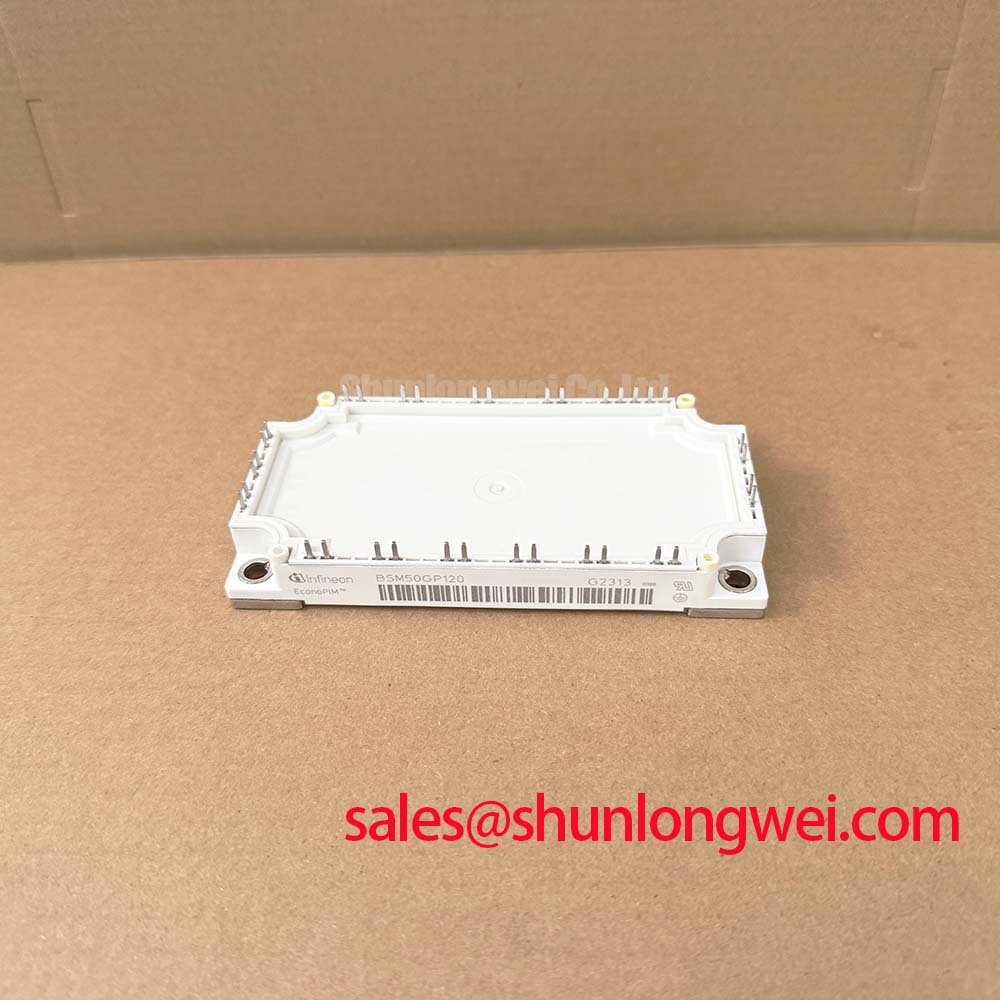
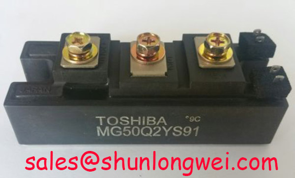
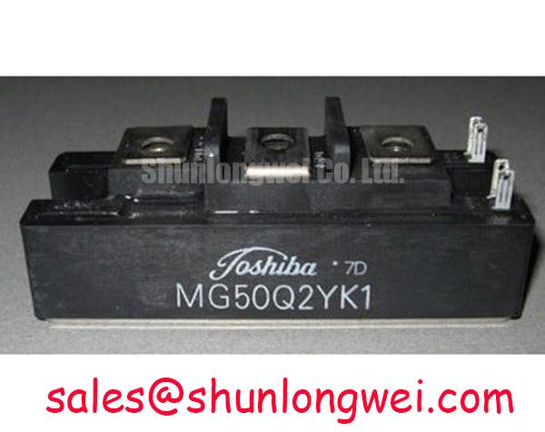
With the power removed and the DC link safely discharged, verify the installed module marking, terminal condition, heatsink contact area, and wiring orientation before evaluating the MG50Q2YK1 in circuit. This Toshiba power module is officially rated at 1200 V and 50 A, supplied in a Toshiba Module housing. Those are the confirmed product ratings available for this model and should be checked against the original equipment documentation before any replacement or recommissioning work.
| Parameter | Official Specification |
|---|---|
| Manufacturer | Toshiba |
| Model | MG50Q2YK1 |
| Collector Emitter Voltage Rating | 1200 V |
| Current Rating | 50 A |
| Package | Toshiba Module |
A module replacement should begin with the equipment’s own electrical boundary checks rather than an assumption that the voltage and current markings alone define interchangeability. The 1200 V voltage rating and 50 A current rating are Official Specifications for the MG50Q2YK1, but the operating DC bus, switching frequency, cooling condition, gate driver arrangement, protection thresholds, and load profile belong to the complete converter system. Engineers should compare these conditions with the original equipment documentation and the applicable Toshiba technical data before energizing the power stage.
In power assemblies that use parallel semiconductor paths, static and dynamic current sharing are separate issues. A positive temperature coefficient of on state voltage can support static current redistribution in some IGBT operating regions, but whether that behavior applies at the intended load, temperature, and gate condition must be verified from the relevant manufacturer curves. It should not be treated as a universal guarantee for the MG50Q2YK1 because the available official data here does not define its VCE(sat) characteristics, temperature coefficient, or switching behavior.
Dynamic sharing is usually more sensitive to external construction than static sharing. Gate leads that differ in length, return path, resistor placement, or driver reference can cause one switching position to react before another. This can create uneven switching stress even where the current path appears symmetrical on a schematic. As a Design Consideration, keep the gate drive loop compact, use equivalent routing where equivalent devices are intended to switch together, and return each gate driver signal through a controlled reference path. Oscilloscope measurements should be taken with an appropriate probing method so that apparent ringing from the probe arrangement is not mistaken for a real gate voltage event.
Field troubleshooting is more reliable when the investigation separates a power fault from a control fault. Inspect terminal fasteners for movement, discoloration, heat affected insulation, or cable strain. Then compare the gate command waveform, collector voltage transition, and load current against a known healthy channel where possible. A repeated protective shutdown may indicate an imbalance, an unstable gate reference, an overloaded process condition, or a protection circuit response. It does not by itself identify one failed component.
For repair planning, the linked MG100Q1ZS40 can be reviewed as another Toshiba module listing, but it must not be considered a direct substitute without a complete comparison of circuit function, package mechanics, pin arrangement, driver requirements, thermal behavior, and all manufacturer specifications. A higher nominal current figure alone does not establish compatibility with an existing inverter welder or induction heating power supply.
⚠️ Maintenance Note: Monitor terminal and heatsink contact temperature during normal production duty, then correct airflow restrictions and loose mechanical interfaces before they develop into intermittent converter trips.
Field Diagnostics & Commissioning: Atmospheric Neutron Radiation Considerations in 1200 V MG50Q2YK1 Topologies
For installations at elevated locations, it is appropriate to document site altitude, cabinet temperature, cooling performance, DC bus behavior, and protective trip history during commissioning. Atmospheric neutron exposure and single event burnout are high risk reliability subjects, and no FIT rate, altitude derating curve, or single event burnout limit is stated in the supplied MG50Q2YK1 specifications. A precise failure rate or a permitted bus voltage reduction cannot be responsibly calculated from the confirmed 1200 V and 50 A ratings alone.
Design Consideration: where altitude or site environment is a concern, the system engineer should obtain manufacturer supported reliability information for the exact device family and evaluate the complete electrical stress profile. The review should include the real DC bus maximum, switching overshoot, transient clamping response, thermal condition, enclosure environment, and protective reaction time. This approach avoids assigning a generic cosmic ray or altitude value to a specific module without documented support.
Commissioning work should also distinguish environmental reliability from ordinary thermal interface deterioration. Remove dust from fins, fan guards, filters, and cabinet air passages before judging the condition of the module. A blocked air route can elevate thermal stress and cause protection events that resemble an electrical defect. Examine the heatsink face for corrosion, embedded debris, flatness concerns, and old thermal material that has hardened, migrated, or become patchy.
As a General Industry Design Consideration, a thin and uniform thermal interface material layer is commonly targeted around 50 to 80 μm when the selected material, surface condition, and assembly process support it. This is not an official MG50Q2YK1 requirement. The actual interface thickness, mounting hardware, screw torque, tightening sequence, and heatsink specification must be determined from the module drawing, equipment manual, and thermal validation results. A cross pattern tightening sequence can help distribute mounting pressure consistently when the mechanical design calls for multiple mounting points.
After reassembly, record baseline temperatures and waveforms under controlled loading rather than immediately returning the equipment to maximum duty. Observe whether cooling fans start correctly, whether airflow passes through the intended path, and whether condensation can form during cold starts or shutdown periods. Moisture control is particularly relevant where equipment moves between warm production spaces and cooler storage conditions. There is no basis in the provided module data for assigning a condensation tolerance to this model, so enclosure sealing and environmental control remain system level decisions.
Long term thermal management depends on the complete stack from semiconductor case to heatsink and airflow path. Engineers reviewing broader cooling architecture can consult The Advanced Thermal Management Revolution for contextual discussion of thermal management approaches. That resource supports system level study and does not replace the MG50Q2YK1 manufacturer documentation or equipment specific thermal measurements.
Transient Dynamics & Electrical Design: Suppressing Cres Induced Gate Voltage Spikes on MG50Q2YK1
Before changing gate components, capture the gate to emitter voltage at the module terminals during the switching event, while also observing collector voltage and load current. The objective is to determine whether an unwanted gate rise coincides with a fast collector voltage transition, a shared emitter path disturbance, a driver supply movement, or measurement artefact. Without official gate charge, capacitance, gate threshold, and switching test conditions for the MG50Q2YK1, a numerical gate resistor, Miller clamp setting, or negative gate bias must not be prescribed for this model.
During a collector voltage transition, capacitive coupling through the device can introduce charge into the gate circuit. If the turn off gate path has excessive impedance, the induced voltage may move the gate toward conduction and create a cross conduction risk in a bridge leg. A dedicated low impedance turn off path or an active Miller clamp can be evaluated as an Engineering Recommendation where the driver supports that function. The final arrangement must be tested in the assembled power stage, including its actual busbar geometry, driver location, current level, temperature, and switching frequency.
Negative gate bias is also a system specific choice, not an Official Specification stated for this module. The driver supply range, isolation arrangement, gate oxide limits, protection behavior, and semiconductor manufacturer guidance must all be reviewed before its use. Selecting a negative bias value from a generic IGBT design note can create a new stress condition if it is incompatible with the module or its driver. Engineers should verify the permitted gate voltage range from the original Toshiba documentation and validate both normal switching and fault shutdown waveforms.
For inverter welder and medium frequency induction heating equipment, the resonant network and switching topology affect the stress seen by each power switch. In circuits using resonant operation, voltage and current may transition under conditions different from hard switched converters. The background principles of zero voltage switching resonant converters can help frame a topology review, but the converter’s actual timing, load variation, and protective limits require direct measurement.
When a repaired unit shows irregular switching, first compare gate command timing between bridge positions, inspect driver supply decoupling and reference integrity, and check whether control cables run alongside high current conductors. Repositioning wiring or restoring a damaged return connection may reduce interference, but the result should be confirmed by measured waveforms rather than inferred from a change in audible noise or fault frequency.
MG50Q2YK1 Thermal Electrical Optimization: Planar Symmetrical Busbar Geometry and Practical Tuning
DC link and switching loop geometry should be reviewed whenever the MG50Q2YK1 is fitted into a repaired or modified power assembly. During turn off, the measured peak device voltage is influenced by the DC bus voltage plus the inductive contribution associated with loop inductance and changing current. Reducing the loop area helps suppress inductive overshoot, but the acceptable geometry, capacitor placement, snubber selection, and peak margin must be determined through system testing against the actual DC link voltage and switching waveform.
Planar, closely coupled busbar arrangements are often considered where high current paths require controlled inductance. The useful principle is to keep outgoing and return current paths physically close and arranged consistently across parallel positions. This is a Design Consideration rather than an official MG50Q2YK1 package requirement. The module drawing and existing equipment layout should govern terminal clearances, conductor orientation, creepage requirements, mounting access, and serviceability.
Snubber capacitors and clamping circuits should be treated as parts of the converter, not as universal accessories selected from the IGBT voltage and current ratings. Their value, voltage capability, pulse current behavior, physical position, and damping network must be established from measured ringing frequency, energy, repetition conditions, and allowable component stress. A capacitor added with long interconnects may have limited influence on the local switching loop, while an incorrectly selected damping network can increase dissipation or change the protection response.
In regenerative operating conditions, a braking chopper and braking resistor may be used by the overall drive system to absorb returned energy. Whether such a circuit is present, how it is controlled, and how much energy it can dissipate are equipment level characteristics. The MG50Q2YK1 official ratings do not establish braking resistor capacity, chopper duty capability, or a safe regeneration setting. Maintenance teams should verify the original power schematic, resistor condition, control feedback path, and protection records before attributing DC bus excursions to the IGBT module.
Practical tuning ends with repeatable verification. Confirm that busbar and gate wiring are secure, inspect thermal material at planned maintenance intervals, remove conductive dust, and measure switching behavior under controlled operating states. Check the DC bus during load transitions, verify that protective circuits respond as intended, and compare results with the equipment’s accepted baseline. This provides a defensible basis for returning a 1200 V, 50 A MG50Q2YK1 installation to service without assigning unsupported electrical or reliability limits to the module.