Content last revised on September 16, 2026
Assembly Integrity and Layout Architecture for Galvanic Gate Drive Isolation
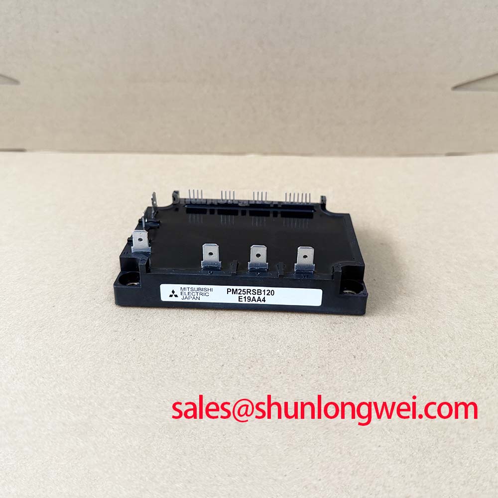
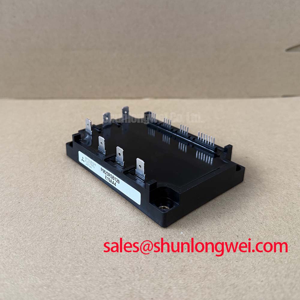
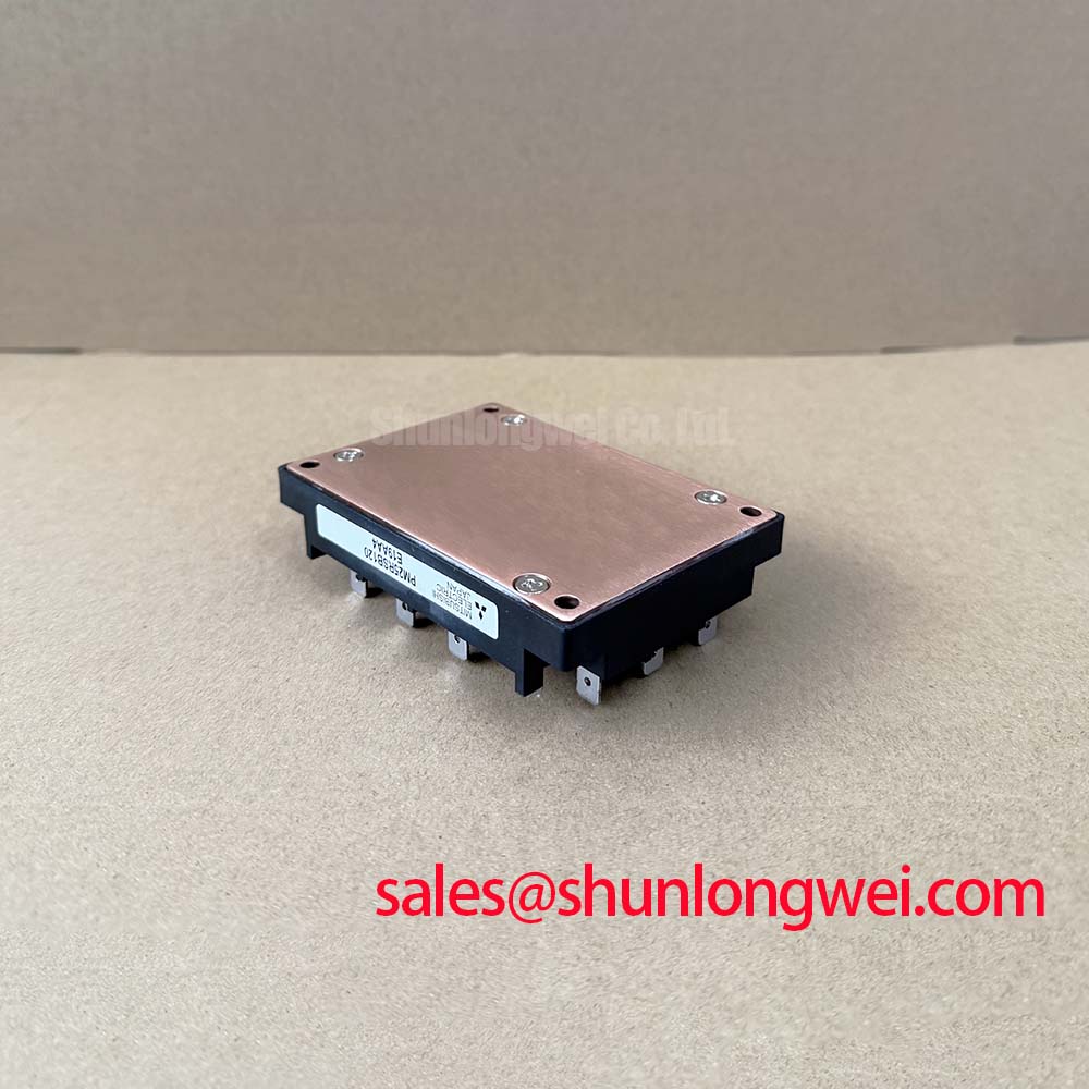
The PM25RSB120 is evaluated as a 1200 V, 25 A Mitsubishi Electric IPM with a specified control supply range of 15 V to 20 V. The published isolation rating is 2500 V at 60 Hz for 1 minute. This rating is an official specification for the stated test condition; it should not be reinterpreted as a complete system insulation or reinforced insulation certification. The finished drive assembly still requires its own creepage, clearance, pollution, enclosure, and safety assessment.
When the module is installed in a light industrial automation inverter or a multi joint robotic articulator drive, the gate drive barrier and the power switching area should be treated as separate electrical domains. Designers should keep high dv dt switching nodes away from control traces, feedback wiring, communication lines, and connector shields. The exact clearance and creepage distances must be selected from the working voltage, pollution environment, insulation system, material group, altitude, and applicable equipment standard rather than assigned from the module rating alone.
The requested reinforced isolation and common mode transient immunity values are system level design targets, not official PM25RSB120 ratings provided here. Therefore, the gate driver or digital isolator selected for the control board should be checked against its own certified isolation and CMTI data. A suitable driver layout uses a compact gate loop, controlled return path, and minimal exposed copper across the isolation boundary. If a control pulse appears at the wrong switching interval, compare the driver input and output with an oscilloscope, inspect the isolated power return, and check whether the event follows the power commutation edge.
A MOV based overvoltage network may be evaluated across the relevant supply or DC link path as a Design Consideration. Its voltage rating, energy capability, clamping behavior, fusing, and coordination with other suppression parts must be determined from the actual bus voltage and transient waveform. The MOV should not be treated as a substitute for a correctly laid out commutation loop. Measure the switching overshoot at the module terminals with a suitable probing method, then verify that the peak remains within the approved operating boundary of the complete power stage.
The Mitsubishi Electric DIPIPM Bootstrap Circuit Design note provides relevant manufacturer guidance for bootstrap based high side drive arrangements. It should be used to verify bootstrap charging, duty cycle limitations, capacitor selection, and control timing where that topology is present. The PM25RSB120 control supply range remains the product specific reference supplied for this page.
💡 Bench Tip: Use ESD protection, keep the module unpowered during cold state comparison, and compare diode mode readings with a known good unit using the same meter polarity and lead arrangement.
PM25RSB120 Operational Boundaries and Gate Drive Loop Geometry
Before connecting a replacement module, identify the original board’s power terminals, control terminals, brake path, and auxiliary return arrangement from the equipment documentation. The supplied PM25RSB120 data confirms inverter current and brake current ratings of 25 A DC, but it does not provide a terminal drawing in the supplied parameter set. Terminal identity and polarity must therefore be confirmed against the original Mitsubishi Electric documentation or the equipment schematic rather than inferred from physical position.
In a practical incoming test, the meter diode function can help identify unexpected conduction paths after the module has been isolated from the driver board and DC link. Test results are only comparative evidence because internal semiconductor paths, parallel components on the board, meter current, and charge stored in capacitors can influence the reading. A low resistance reading between power terminals should be investigated with the module removed from surrounding circuitry. Do not apply an external gate or control supply until the terminal map and required control sequence have been verified.
Separating the auxiliary emitter return from the high current emitter route is a Design Consideration where the module provides a corresponding auxiliary connection. The purpose is to reduce mutual coupling between the gate reference and the main current path. The available PM25RSB120 terminal arrangement should be confirmed from the manufacturer’s mechanical and electrical drawing before calling any terminal a Kelvin emitter. If the equipment wiring does not provide a separate auxiliary return, the system designer should review the actual current path, parasitic inductance, and driver reference behavior rather than adding an unverified connection.
Gate loop geometry should be kept compact and routed as a controlled pair from the driver output to the applicable gate and return terminals. Avoid sharing the gate return with a high di dt power conductor. During troubleshooting, check the gate to emitter waveform at the module pins, not several centimeters away on the driver board. Ringing, inconsistent turn off behavior, or a gate waveform that changes with cable position may indicate parasitic coupling or an impedance mismatch. Verify the observation against a known good signal path and review probe ground technique before changing gate components.
Any gate resistance, damping network, negative bias, desaturation protection, and dead time are system determined. They depend on the switching frequency, driver capability, load current, bus impedance, thermal condition, and measured switching waveform. The PM25RSB120 official data supplied here does not authorize a universal gate resistor or fixed protection setting. A commissioning engineer should tune these values from measured gate voltage, collector emitter voltage, current transition, and fault response while maintaining the module’s published electrical and thermal limits.
For a neutral comparison during maintenance planning, engineers may review SKIIP37AC12T4V1 as another power module reference. Electrical interchangeability is not established by current or voltage labels alone. Package geometry, terminal assignment, control logic, isolation data, thermal interface, protection behavior, and mechanical mounting must all be checked before any substitution is considered.
Symmetrical Busbar Geometry for High Current and Brake Paths
The inverter and brake current ratings are both specified as 25 A DC. These values identify the stated product ratings, not an automatic guarantee for every switching frequency, case temperature, overload profile, cooling arrangement, or duty cycle. When integrating the module into an industrial drive, the system engineer should calculate conduction and switching losses from the actual operating waveform and then verify junction temperature through an approved thermal model and measurement method.
Symmetrical busbar geometry is an Engineering Recommendation when more than one parallel current path or more than one switching device is used in the system. Equalizing the electrical path length and impedance helps prevent one path from carrying disproportionate current. The same principle applies to the return path: avoid placing a high current conductor beside sensitive control wiring where magnetic or electric coupling can affect the gate signal.
Static current sharing between parallel IGBT paths may benefit from the positive temperature coefficient commonly associated with the on state voltage of IGBT devices, but the effect should not be treated as sufficient protection against all imbalance. Dynamic sharing is influenced by gate loop inductance, driver timing, stray inductance, device parameter spread, busbar geometry, and thermal gradients. If parallel operation is being evaluated, designers should measure current in each path during startup, steady state, braking, and fault interruption, then verify the peak values against the system’s thermal and electrical limits.
The brake branch deserves the same inspection as the inverter path because its official DC collector current rating is also 25 A. Confirm the brake resistor, switching frequency, pulse duration, cooling, and fault isolation independently. A brake circuit that appears satisfactory during short bench operation may produce a different thermal result during repeated deceleration. Record the DC link voltage, brake current waveform, switching interval, and module case temperature during a representative equipment cycle.
For overvoltage control, the MOV network, DC link capacitor bank, snubber arrangement, cable inductance, and braking system should be reviewed as one network. Component placement should minimize the power commutation loop and keep suppression components electrically close to the terminals they protect. The correct suppression voltage is system determined and must account for normal bus voltage, tolerance, regenerative rise, and the module’s 1200 V Vces rating. Confirm the result with a differential high voltage probe and a controlled switching test.
When a repaired drive shows abnormal heating or intermittent overcurrent, inspect busbar flatness, terminal seating, joint pressure, contamination, and the symmetry of parallel copper paths. Then compare phase current and gate waveforms rather than assigning the symptom to a single component. The PM25RSB120 junction temperature range of −20 °C to +150 °C provides the official boundary supplied here, while the allowable case temperature and heatsink condition must be established from the complete thermal design.
Voltage Derating and Environmental Robustness for High Altitude Operation
The PM25RSB120 has an official 1200 V collector emitter voltage rating and an isolation specification of 2500 V at 60 Hz for 1 minute. These values should be entered into the equipment verification record exactly as specified. They do not provide a field failure rate, FIT value, cosmic ray immunity value, or guaranteed operating altitude. No numerical Single Event Burnout rate should be assigned without an authoritative device study, qualification report, or manufacturer application document covering the actual voltage, altitude, waveform, and population.
At elevated installation sites, reduced air pressure can affect external insulation clearances and thermal performance, while terrestrial neutron exposure may be included in a system reliability assessment for high voltage power semiconductors. The appropriate response is a Design Consideration: review the applicable altitude correction and insulation standard, examine the DC link operating distribution, and ask the device manufacturer for any relevant high altitude or cosmic ray qualification information. A generic FIT estimate would not be technically defensible from the product ratings listed here.
Voltage derating should be established from measured maximum DC link voltage, regenerative events, switching overshoot, tolerance, and the approved application limits. The system engineer should verify peak collector emitter voltage at the module terminals under worst case load and commutation conditions. If the result leaves insufficient engineering margin, possible system level actions include reducing the operating bus voltage, improving the clamp network, changing commutation layout, or selecting a device with a different voltage class. The suitable action depends on the equipment architecture and must be validated by testing.
External insulation inspection is equally important. Check the distance between high voltage copper, control traces, mounting hardware, heatsink surfaces, and accessible metalwork. Creepage and clearance are affected by board contamination, condensation, coating, slot geometry, and enclosure design. The module’s isolation test rating should not be used as a replacement for a complete hipot and insulation resistance procedure defined for the finished drive.
For technology background, the engineering discussion in Unlocking Efficiency in Industrial Drives can help engineers place switching efficiency and drive behavior in a wider power semiconductor context. Mitsubishi Electric also maintains a separate reference area for SiC Power Modules and SBDs; that material should be treated as technology information, not as evidence that the PM25RSB120 is a SiC device or that it is interchangeable with a SiC module.
For field troubleshooting, document the equipment altitude, enclosure condition, DC link voltage, switching waveform, cooling path, fault history, and the cold state electrical comparison. This evidence supports a controlled engineering decision without attributing a failure to cosmic radiation, insulation breakdown, or thermal overstress before the relevant measurements and source data are available.