
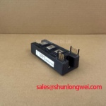
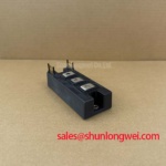
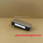
Content last revised on September 15, 2026
PM25DSA120 Thermal Electrical Optimization for Long Motor Lead Reflected Wave Voltage
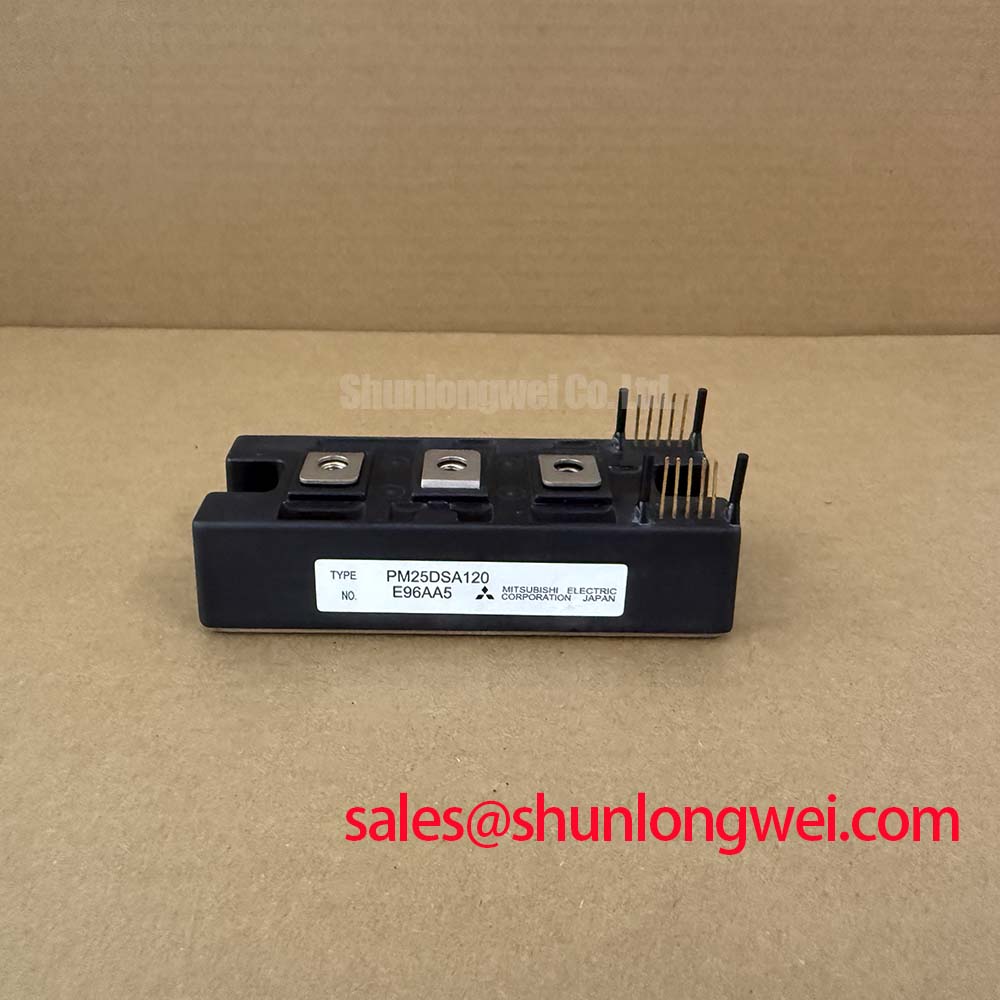
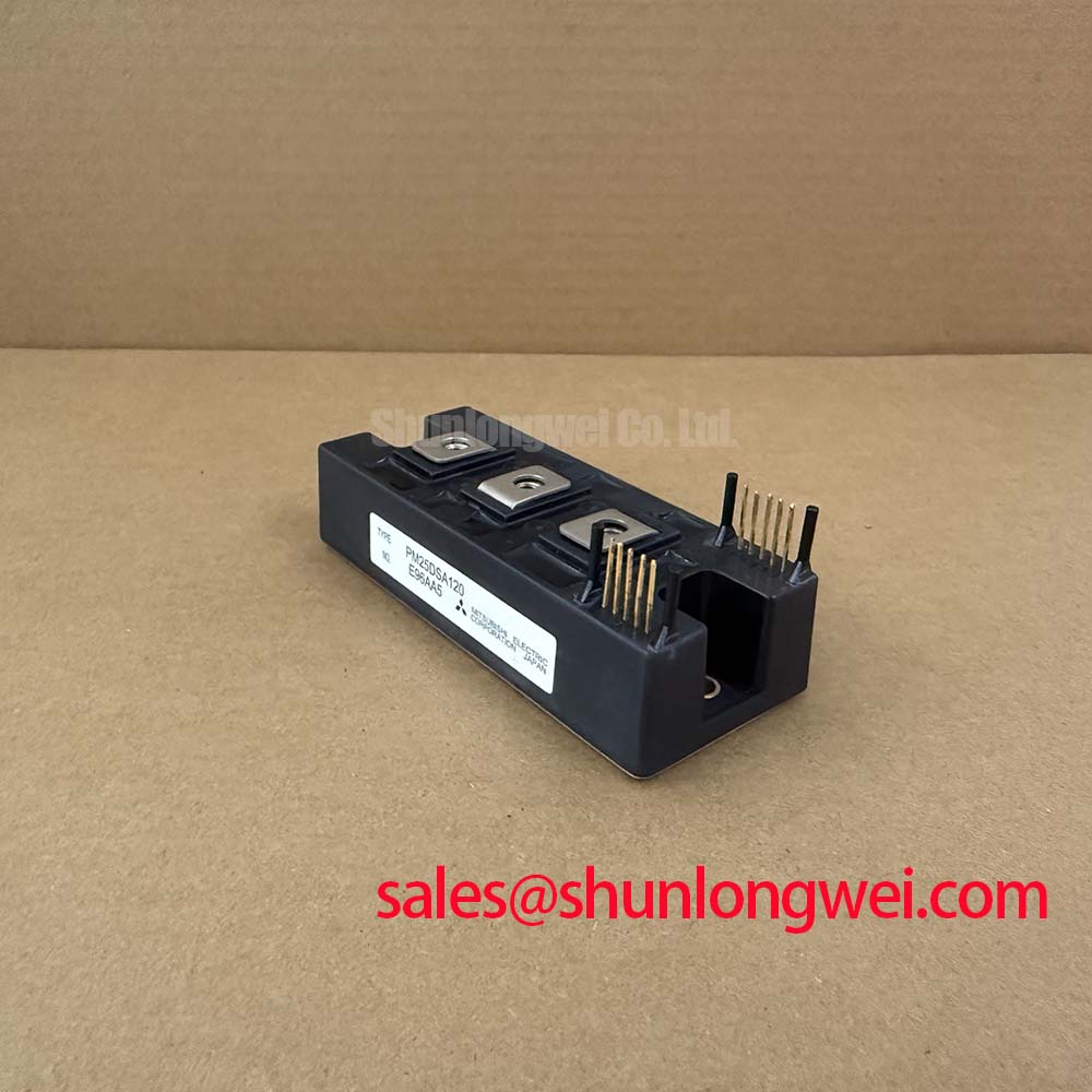
Before connecting a replacement, isolate the drive, protect the module from ESD, and verify the PM25DSA120 terminal markings against the original inverter wiring. Record the cold resistance and diode test behavior of the power terminals before applying a control supply, then compare the nameplate limits with the circuit DC bus, motor current, and switching conditions.
| Parameter | Symbol | Official Specification |
|---|---|---|
| Collector emitter voltage | VCES | 1200 V |
| Continuous collector current at TC = 25 °C | IC | 25 A |
| Collector emitter saturation voltage | VCE(sat) | 2.7 V typical, 3.4 V maximum |
| Recommended switching frequency | fsw | Up to 20 kHz |
| Over current trip level | OC | 38 A typical |
| Control supply under voltage lockout | UVLO | 12.5 V typical |
| IGBT junction to case thermal resistance | Rth(j-c) | 1.5 °C/W maximum |
| Isolation voltage for one minute AC test | Viso | 2500 Vrms |
The table contains official product data supplied for this Mitsubishi Electric IPM. Gate driver timing, short circuit withstand duration, internal terminal arrangement, surge current capability, and detailed package dimensions should be checked against the original manufacturer documentation before a production replacement is approved.
In a compact industrial inverter or high speed CNC spindle drive, long motor cables can behave as transmission lines rather than simple resistive connections. Impedance mismatch at the motor terminals can return a portion of the switching edge toward the inverter. This reflected energy can produce a voltage at the motor terminals approaching twice the incident voltage in some cable and termination conditions, creating overshoot that may substantially increase voltage stress relative to the DC bus. That behavior is a system design consideration, not an additional voltage rating for the 1200 V PM25DSA120.
When evaluating a long lead installation, measure the switching waveform at both the IPM output and the motor end with a suitably rated differential probe. Probe placement, probe loop area, grounding method, cable shield termination, and oscilloscope bandwidth can materially change the observed result. Designers should verify the peak collector emitter voltage against the actual DC link voltage during acceleration, deceleration, regenerative operation, and commanded stop conditions.
An output reactor, common mode choke, dv/dt filter, or motor terminal filter may reduce edge energy, conducted common-mode current, or voltage stress, depending on its topology and installation. The correct device and location are determined by the motor cable length, cable impedance, switching frequency, motor insulation system, leakage current limits, and drive control response. Avoid selecting a filter only from the inverter current rating. Confirm that the filter does not create an undesirable resonance with the DC link, motor inductance, or cable capacitance.
The official switching frequency reference for this unit is up to 20 kHz. This value should be treated as a product application reference rather than a complete thermal design guarantee. Actual junction temperature depends on current waveform, modulation method, switching loss, case temperature, cooling interface, and enclosure airflow. The specified Rth(j-c) of 1.5 °C/W maximum provides the thermal path reference from junction to case, while the heatsink and thermal interface remain system responsibilities.
For regenerative braking, the braking resistor and chopper control must be evaluated with the complete DC bus energy profile. The resistor absorbs energy during deceleration, but its pulse rating, average power, thermal recovery, and enclosure ventilation are not specified by the PM25DSA120 data listed here. Measure the bus rise during the fastest expected stop and verify that the chopper control does not repeatedly approach the inverter voltage limit.
PM25DSA120 Circuit Protection and Symmetrical Busbar Geometry
Use the cold test as an incoming reference, not as a substitute for a powered functional test. With the module disconnected, identify the power terminals from the approved circuit drawing and check diode direction using a calibrated meter. A forward reading on an antiparallel path may be expected, while an unexpected low impedance in both polarities may justify comparison with a known good unit and further isolation testing. Do not assign a fixed pass or fail voltage to a handheld diode test unless the manufacturer provides that method and limit.
The listed VCE(sat) is 2.7 V typical and 3.4 V maximum. This is an official static specification under defined test conditions, not a universal field voltage at every current and temperature. For thermal review, use the manufacturer test conditions and the actual load waveform. A rising saturation voltage during operation can have several causes, including current increase, junction temperature, driver behavior, supply droop, or measurement error.
Parallel current paths should be laid out with similar electrical length and comparable conductor geometry. This is a Design Consideration for reducing unequal stray inductance and dynamic current imbalance. The busbar should avoid narrow necks near high current terminals, abrupt plane transitions, and unnecessary commutation loop area. The final geometry must be validated with current probes and switching waveforms rather than inferred from visual symmetry alone.
Static current sharing can benefit from the positive temperature behavior commonly associated with IGBT conduction characteristics, but dynamic sharing is also governed by gate resistance, driver propagation delay, emitter inductance, busbar inductance, and layout coupling. Designers should match the gate loop routing for each switching position and verify turn on and turn off timing under the highest anticipated current.
The official over current trip reference is 38 A typical. Because this is a typical threshold, protection coordination should include sensing tolerance, delay, temperature, wiring inductance, and the response of the upstream controller. Dead time should be sufficient to prevent cross conduction between complementary devices, but excessive dead time can increase diode conduction and switching loss. The appropriate dead time is system determined through double pulse or inverter switching tests.
A neutral comparison point for engineers reviewing another power stage is SKIIP37AC12T4V1. It should be treated as a separate product reference, not as an automatic substitute. Pin compatibility, gate drive requirements, protection behavior, thermal interface, mechanical mounting, and electrical ratings must all be confirmed independently.
Benchtop Waveform Tuning and Common Mode Transient Immunity
The control supply should be checked before any switching command is enabled. The published UVLO threshold is 12.5 V typical, so the driver supply should be observed at the module pins during gate activity rather than measured only at the power supply output. Supply wiring inductance and local decoupling can cause a transient dip that is invisible at a remote test point.
Do not infer a reinforced isolation barrier or a specific common mode transient immunity value from the IPM category alone. The supplied official data specifies Viso = 2500 Vrms for an AC one minute isolation test. This value must not be rewritten as a greater than 5 kV barrier or a CMTI rating above 100 kV per microsecond without a manufacturer source. The insulation test voltage, creepage, clearance, transient performance, and certification status are different engineering properties.
During bench testing, monitor the gate emitter waveform, control supply, switching node, and fault output together. A narrow unwanted gate pulse may result from common mode coupling, an inadequate return path, excessive parasitic inductance, driver supply disturbance, or probe interaction. Compare the suspect channel with the corresponding reference channel and repeat the measurement with a reduced probe loop.
Gate loop routing should keep high dv/dt power nodes away from sensitive control traces. Minimize parasitic loop inductance to reduce turn off overshoot, then verify the peak voltage and gate voltage margin during the actual switching event. If high frequency ringing remains, a ferrite component may be considered after impedance and loss testing. Background information on high frequency attenuation is available through Ferrite bead high frequency parasitic ringing attenuation.
The driver supply and bootstrap network, where used by the particular system, must be checked against the original gate driver design. Bootstrap capacitor charging time, high frequency charge removal, diode reverse recovery, duty cycle, and low side refresh intervals are system dependent. The PM25DSA120 page data supplied here does not establish a capacitor value, diode type, or guaranteed high side on time.
Loop gain and control stability should also be assessed after adding an output filter or braking network. A filter can alter the plant response and create a control interaction that is not visible in a static resistance test. Engineers can use a Bode plot frequency response and gain margin reference when evaluating this behavior, while final acceptance should rely on measurements from the complete inverter.
Bench Tip: Keep the module and disconnected control cable at the same ESD protected workbench potential, and record a cold reference before repeating any powered waveform test.
Field Diagnostics and Commissioning of Desaturation Detection Topologies
Commissioning should begin with the DC bus disabled and the gate command inhibited. Check terminal polarity, mechanical seating, thermal contact, control supply rise, fault input state, and isolation test documentation in a controlled order. The module’s 2500 Vrms isolation specification for one minute is an official test rating under stated conditions; it does not define an unlimited production hipot procedure or guarantee the insulation of the assembled inverter.
The supplied product parameters identify an over current trip level of 38 A typical, but they do not provide a verified type I or type II short circuit response time, a desaturation blanking interval, or a short circuit safe operating area duration. Claims such as detection within 10 microseconds should therefore be treated as unverified for this product page. The system designer should obtain the applicable Mitsubishi Electric application data before implementing a protection sequence around those values.
Where an external desaturation or collector voltage monitor is used, place the sensing path close to the switching device and validate it during controlled fault testing. A two stage soft turn off may reduce the rate of current interruption and the resulting inductive overvoltage, but its delay, gate clamp behavior, fault latch logic, and reset conditions must be selected from the complete driver and protection architecture.
During a fault investigation, capture the gate command, gate emitter voltage, collector emitter voltage, phase current, DC link voltage, and fault signal on one time base. A fault indication without a corresponding power waveform does not identify the failed mechanism. Possible contributors include current transformer saturation, sensor delay, driver supply collapse, wiring inductance, an incorrect gate reference, filter resonance, or an actual semiconductor fault.
For a system that uses a separate rectifier or front end, engineers may review CM100DY 12E as a related topology reference. It is not a stated replacement for the PM25DSA120. Confirm voltage class, current duty, commutation path, cooling method, terminal arrangement, and controller coordination before considering any cross reference.
Thermal recovery checks should include the case temperature, heatsink temperature, thermal interface condition, mounting flatness, and the transient load history. A thin, continuous thermal interface layer is a Design Consideration, while the correct application method and mounting torque must come from the module documentation and mechanical design. Do not use a generic torque value as a Mitsubishi Electric specification.
For broader evaluation of 1200 V power conversion technologies, the article The 1200 V CoolSiC MOSFET Advantage in Three provides a separate technology reference. Its conclusions should not be transferred directly to the PM25DSA120, whose ratings and switching behavior require product specific verification.