

Content last revised on September 24, 2026
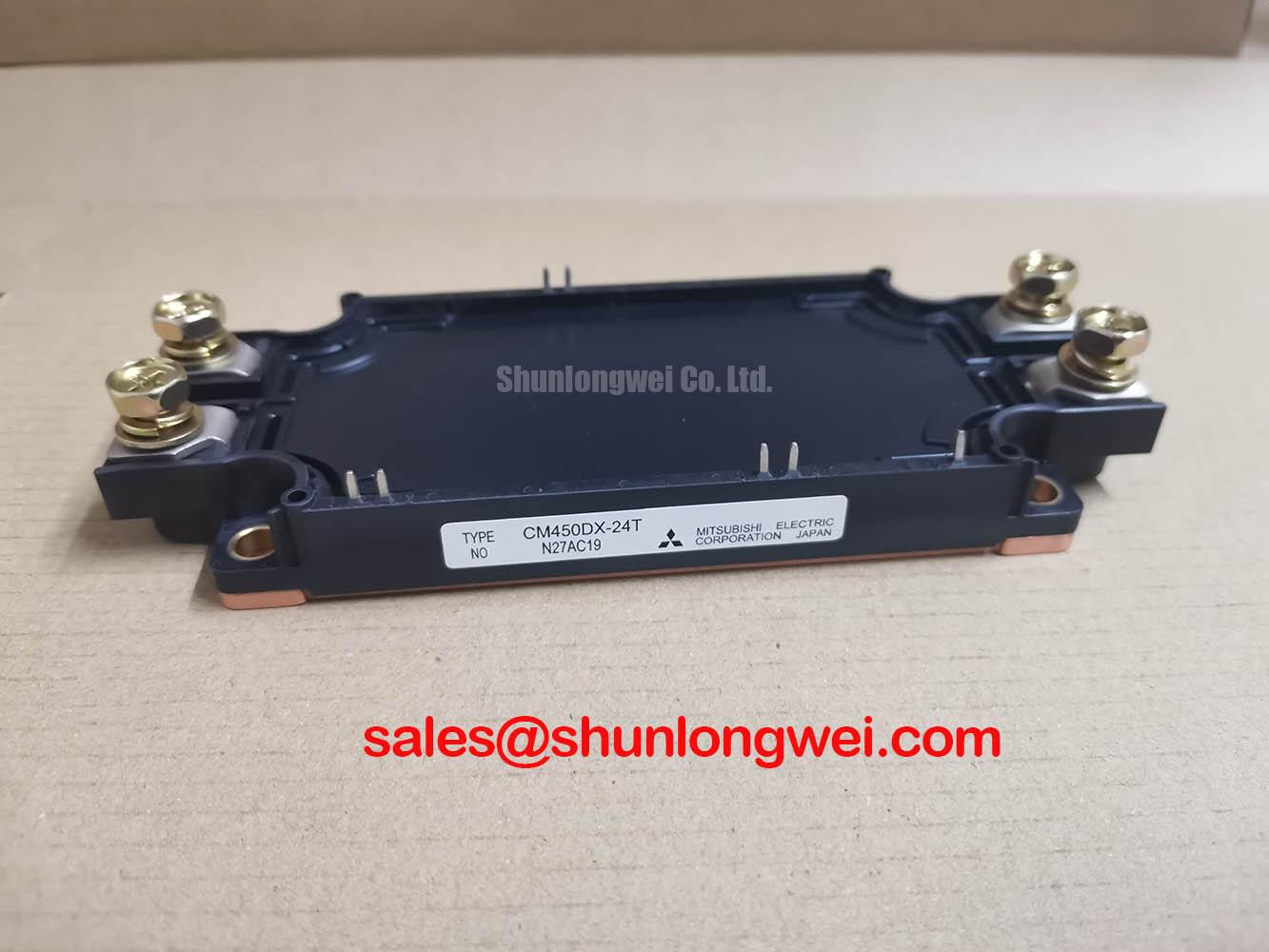
Assembly Integrity and Layout Architecture for the CM450DX-24S1
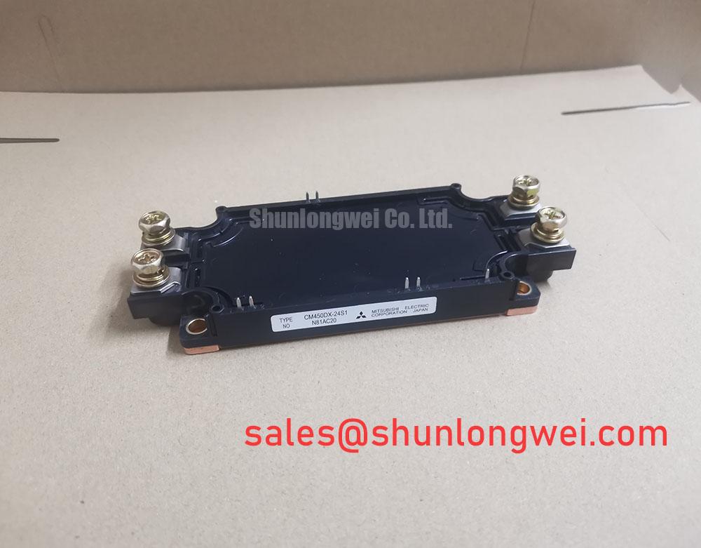
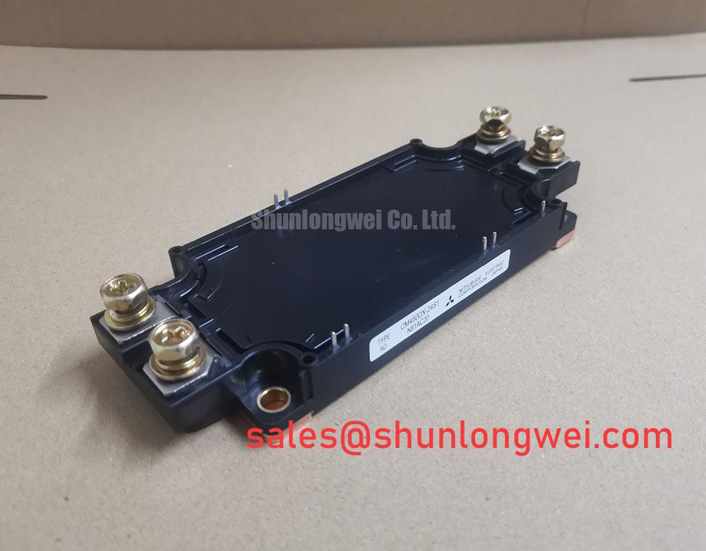
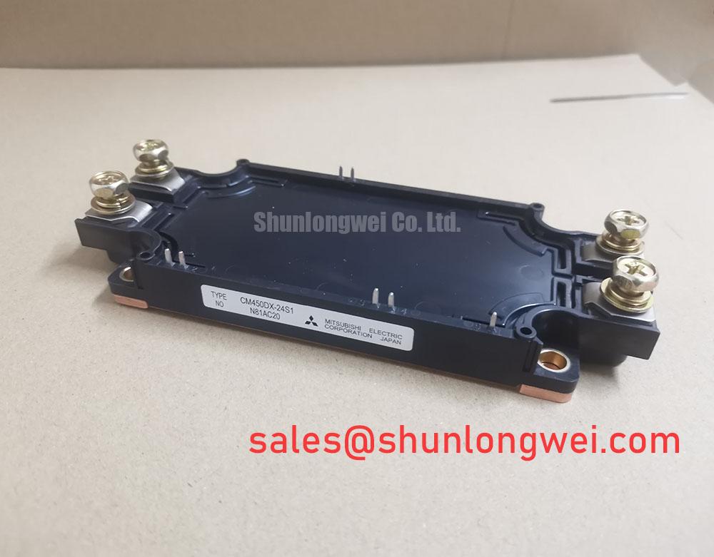
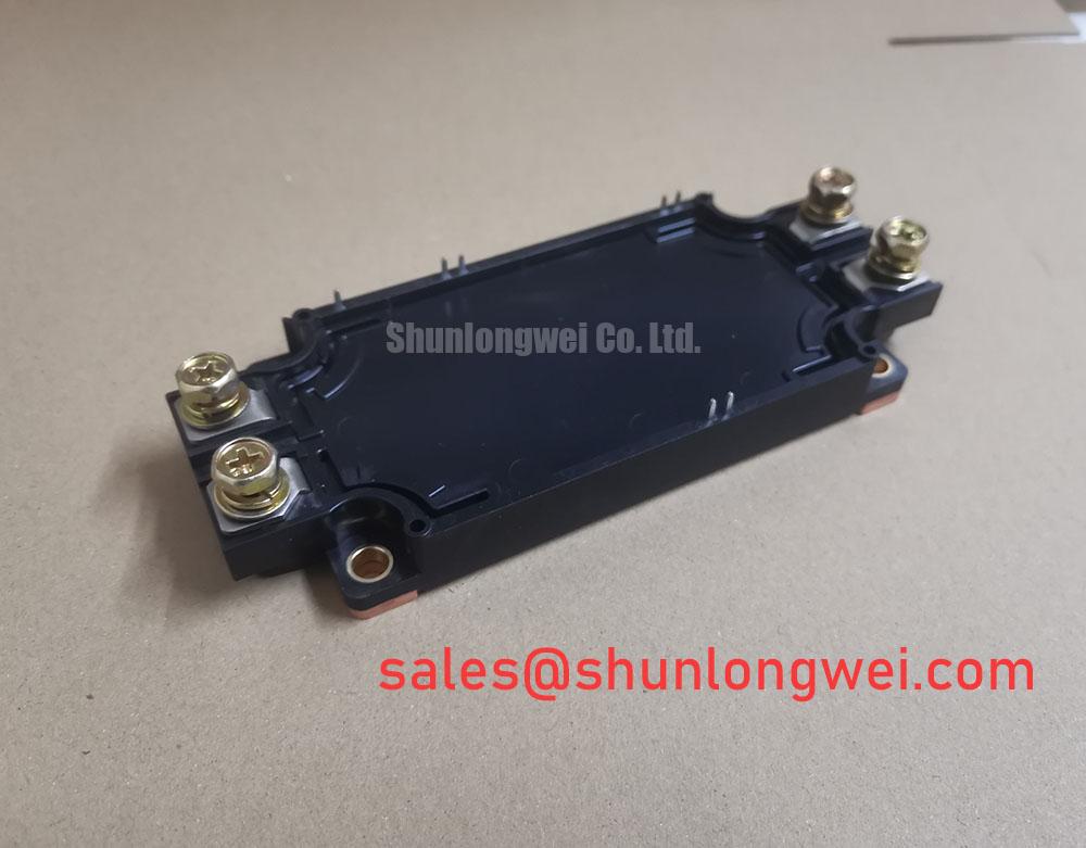
Before fitting the module into a converter, compare the replacement footprint with the original busbar, gate driver, auxiliary terminal, and mounting arrangement. The listed package classification is simply Module; it does not confirm a universal terminal layout for every equipment platform. Use the manufacturer’s terminal drawing for polarity, gate, emitter, collector, auxiliary emitter, and isolation details rather than relying on a visually similar power module.
Design Consideration: the power emitter return and the gate-driver return should be treated as separate current paths whenever the documented terminal arrangement permits it. High collector-emitter current produces voltage across stray inductance and copper resistance. If the gate-return path shares the same high-current section, the driver can sense an unwanted voltage disturbance, which may appear as ringing, uneven switching, or a false turn-on tendency. Keep the gate loop physically compact, route outgoing and return conductors close together, and maintain comparable geometry for complementary switching positions.
For a three-phase converter, the gate-driver boards should be located so that corresponding power paths have similar conductor length, connector construction, and return impedance. Do not assume that equal schematic distance produces equal electrical behavior. Inspect actual copper width, via transitions, connector pins, and busbar bends. Clearance and creepage must be selected from the system working voltage, pollution environment, altitude, insulation system, and applicable safety standard; the module’s 1200.0 V rating alone does not define those PCB distances.
A cold-state incoming test should begin with the DC link fully discharged and the gate terminals protected from static electricity. Use the diode-test function only where the manufacturer’s test method and terminal map support that measurement. Record the polarity and compare forward conduction behavior with a known-good reference of the same part number. A meter reading is a screening observation, not proof of dynamic switching performance or insulation integrity. If the result is unexpected, repeat the test with leads, fixtures, and adjacent circuit paths isolated.
For a neutral comparison point during maintenance planning, engineers may review the FF45017ME4 as a separate high-power module reference. It should not be treated as a drop-in substitute without confirming electrical ratings, terminal geometry, gate requirements, thermal interface, mechanical fit, and protection coordination.
Turn-Off Transient Control and Practical Electrical Tuning
During turn-off testing, use a properly rated differential probe and measure the voltage directly at the module power terminals, not only at a remote DC-link capacitor. The switching overshoot is influenced by DC-link voltage, commutation current, stray inductance, switching speed, probe connection, and busbar geometry. In engineering terms, the peak voltage rises with the inductive contribution associated with stray inductance and current-change rate, so the design team must verify the measured peak against the module rating and the system’s required transient margin.
Engineering Recommendation: minimize the commutation loop area with a closely coupled, symmetrical laminated or planar bus structure where practical. The frequently quoted target of less than 25 nH is not an official parameter supplied here for the CM450DX-24S1, so the final inductance limit must be established by the converter designer through impedance evaluation and switching measurements. Snubber selection also remains system-dependent. A capacitor that reduces overshoot may increase circulating current, switching loss, or resonance, while excessive damping can affect efficiency and thermal loading.
When a controlled turn-off waveform shows ringing, inspect the probe ground arrangement, gate-resistor population, driver return path, DC-link capacitor placement, and busbar joints before changing component values. A gate resistor or RC network should be treated as a typical starting point for bench tuning rather than a guaranteed value for this module. The engineer should change one variable at a time while recording collector-emitter voltage, gate-emitter voltage, current, switching loss, and heat-sink temperature.
Dead-time and interlock are also controlled by the complete gate-driver system. The designer should establish a dead-time buffer that covers driver propagation mismatch, temperature drift, command skew, and measured switching delay. Excessive dead-time can increase diode conduction and recovery stress; insufficient dead-time can permit cross-conduction. Confirm the result at the actual gate terminals of each parallel or complementary switch, especially after cable, connector, and isolated-driver installation.
For broader reference when assessing a 1200 V power-conversion bus, the maintenance team can consult The 1200 V CoolSiC™ MOSFET Advantage in Three. That article concerns a different semiconductor technology and should be used for topology discussion, not as a substitute for the CM450DX-24S1 data.
Thermal Interface Control and Benchtop Waveform Tuning
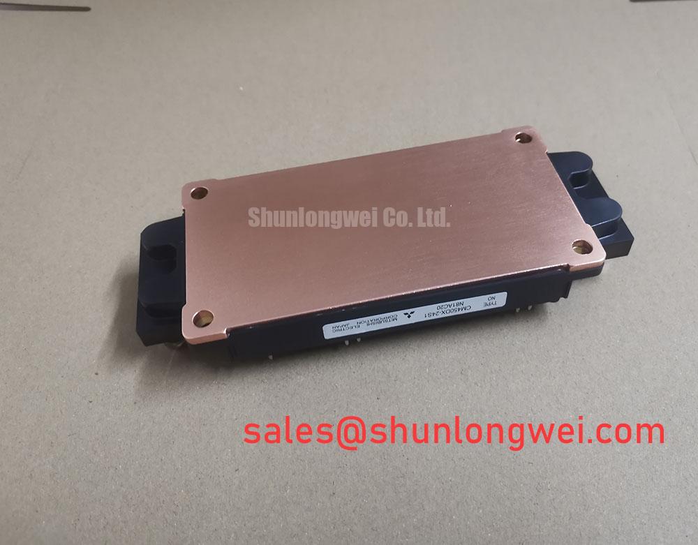
Mechanical installation should start with a clean, flat mounting surface and a checked baseplate. Remove old thermal compound without scratching the contact area, inspect for burrs, and verify that the heat sink does not rock when placed on a reference surface. Thermal interface material thickness is a design variable, not an official CM450DX-24S1 rating. The objective is continuous contact with minimal voiding while avoiding excessive compound that can increase thermal resistance or contaminate nearby insulation.
Apply the selected thermal compound or interface material according to its manufacturer’s process instructions. A thin, even layer is generally a Design Consideration, but the correct thickness depends on surface flatness, material rheology, pressure distribution, and the interface supplier’s data. Do not copy a 50 to 100 micrometre figure as a guaranteed requirement for this module unless it is supported by the selected interface material process and the equipment manufacturer’s mechanical specification.
Use a staged, diagonal tightening sequence so that the module baseplate settles evenly. The correct screw type, washer arrangement, torque, sequence, and final pass must come from the Mitsubishi Electric mechanical documentation or the host equipment service manual. ⚠️ Field Alert: never connect or disconnect gate and power wiring while the DC link or auxiliary supply remains energized, even when the converter appears idle.
After assembly, inspect the interface perimeter for displaced compound and check that the module has not tilted during tightening. Thermal validation should combine heat-sink temperature, case temperature where measurable, switching waveform, load current, and ambient condition. A transient thermal impedance curve, often written as Zth, describes the thermal response to a defined power pulse; it must be taken from the applicable manufacturer data rather than reconstructed from a generic module family.
For a wind turbine full-scale converter, the power stage may experience changing conduction intervals, regeneration, and long-duration thermal cycling. The system integrator should assess the rectifier and inverter control strategy, including conduction angle and grid-current harmonic suppression, at the actual operating point. Passive or active harmonic measures, modulation strategy, line impedance, and filter design determine compliance; the IGBT module alone does not establish grid harmonic performance.
Field Diagnostics and Commissioning for Parallel Current Sharing
When several modules operate in parallel, begin commissioning with low-energy checks of polarity, gate-driver continuity, auxiliary returns, and current-sensor orientation. Confirm that each module receives the intended command and that the driver reference is connected to the correct emitter reference. Compare gate-emitter waveforms at the module terminals rather than at the driver output alone. Unequal delay, loop inductance, connector resistance, or thermal conditions can produce dynamic current imbalance even when the schematic is symmetrical.
Static sharing is influenced by the electrical characteristics of the parallel devices and their operating temperature. A positive temperature coefficient of on-state voltage can support stabilizing current-sharing behavior in suitable operating regions, but this should be treated as a Design Consideration and verified from the applicable output-characteristic curves. It does not remove the need for matched current paths, equal thermal impedance, balanced gate wiring, and individual protection review.
During a controlled load increase, record phase current, module case temperature, gate waveform, collector-emitter voltage, and protection status. If one current trace diverges, inspect busbar resistance, terminal pressure, sensor calibration, driver timing, thermal contact, and the measurement bandwidth before assigning a single cause. An oscilloscope comparison with a known-good phase can help distinguish a control-path difference from a power-path difference.
Fast semiconductor fuses and short-circuit protection must be coordinated with the converter’s actual fault energy. The fuse I²t value, module short-circuit withstand information, gate-driver desaturation response, DC-link capacitance, and clearing time belong to one protection study. Do not infer a safe short-circuit duration from the 450.0 A current rating. The system engineer should verify fault tests, isolation behavior, interlock response, and the required protective device using the applicable Mitsubishi Electric data and the host converter safety design.
For a multi-megawatt onshore or offshore wind turbine converter, enclosure sealing, cooling redundancy, vibration, service access, and grid-code requirements remain equipment-level concerns. The CM450DX-24S1 provides the stated 1200.0 V voltage rating, 450.0 A current rating, and module package classification; final compatibility depends on the complete electrical, mechanical, thermal, and protection review.