

Content last revised on September 10, 2026
Transient Dynamics & Electrical Design: Baseplate Convexity Compensation and Screw on GD200FFX120C6S
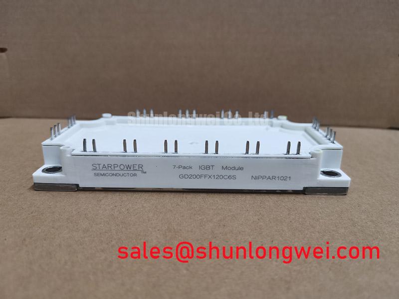
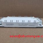
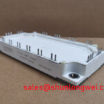
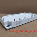
Before fitting the module, isolate the converter, discharge the DC link according to the equipment procedure, inspect the terminal areas and mounting face, then verify that the replacement label identifies GD200FFX120C6S. This StarPower power semiconductor is an IGBT Module rated at 1200 V and 200 A as Official Datasheet Specifications. Confirm the original circuit topology, gate driver interface, mechanical outline, terminal arrangement, cooling assembly, and protection settings against the equipment documentation before installation.
| Parameter | Specification Status |
|---|---|
| Product model | GD200FFX120C6S |
| Manufacturer | StarPower |
| Collector emitter voltage rating | 1200 V Official Datasheet Specification |
| Current rating | 200 A Official Datasheet Specification |
| Package | Module Official Datasheet Specification |
For industrial inverter welder and medium frequency induction heating repairs, the electrical ratings alone do not establish interchangeability. The service team should compare the original module’s circuit function and external connection geometry with the candidate device. Where a parallel review is needed, P546A2005 can be examined as a same class reference model, while its own electrical and mechanical documentation remains the basis for any compatibility decision.
The first thermal task is to inspect the heatsink contact plane rather than assuming a new module will correct an existing overheating issue. Residue from aged thermal compound, embedded debris, corrosion, or local damage can prevent uniform contact across the module base. Clean the mating surface using an approved maintenance process, inspect it under oblique light, and check that the cooling plate is not distorted by prior overtightening or uneven clamping.
Thermal interface material must fill microscopic surface irregularities without becoming a thick insulating layer. A 50 to 100 μm controlled TIM layer is a general industry Design Consideration when the material supplier, flatness condition, and assembly method support that thickness; it is not an official mounting specification for GD200FFX120C6S. The installer should follow the thermal material supplier’s handling guidance and the equipment manufacturer’s mechanical instructions. Excess compound around terminal zones should be removed because contamination can retain dust and make later inspection difficult.
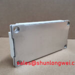
Baseplate curvature is an assembly issue that deserves attention in high duty equipment. A slight mismatch between module and heatsink may leave one region poorly coupled, creating a local thermal gradient even if cabinet airflow appears normal. A practical inspection is to document the old compound transfer pattern when the failed or removed module is lifted from the heatsink. Uneven transfer does not prove one cause, but it gives maintenance staff a useful reason to inspect the cooler plate, clamp sequence, and mounting hardware.
Screws should be engaged by hand first and tightened progressively in a balanced sequence so that the module settles evenly against the heatsink. The applicable torque must come from the original equipment mechanical drawing or the module documentation, because the approved value depends on screw type, thread engagement, washer arrangement, heatsink material, and joint design. ⚠️ Maintenance Note: Recheck terminal and mounting fastener tightness only with the equipment isolated, because a loose high current joint can produce contact heating that is easily mistaken for a semiconductor fault.
Keep power conductors routed so that service access does not force stress into module terminals. This is a Design Consideration, particularly in inverter welders where cable movement and repeated thermal cycling can alter contact pressure over time. During preventive maintenance, inspect heatsink fins, fan direction, duct seals, moisture paths, and signs of condensation. Contact temperature trends are more useful than a single observation, provided they are measured at consistent load and ambient conditions.
Field Diagnostics & Commissioning: DC Link Capacitance Bank Layout and Low ES in GD200FFX120C6S Topologies
When an installed converter shows recurring overvoltage trips, inspect the DC link capacitor bank, laminated conductors, snubber network, and module connections as one switching loop. The peak collector emitter stress rises from the DC link voltage by an inductive term related to loop inductance and current transition rate. This Engineering Calculation principle explains why physically separated capacitors, long bus paths, or asymmetric connections can produce switching waveforms that differ from the expected design behavior.
Designers should minimize parasitic loop inductance to suppress turn off overshoot, then verify peak voltage margins against the actual DC link voltage during switching tests. The required capacitor type, snubber capacitance, damping method, conductor geometry, and measurement bandwidth are determined by the converter topology and validated waveform results. No specific snubber value or busbar inductance limit should be assumed from the 1200 V module rating alone.
For service work, begin with the unpowered checks permitted by the machine procedure. Examine capacitor terminals for heat marks, connector interfaces for discoloration, and busbar surfaces for looseness or contamination. Under controlled commissioning conditions, compare collector emitter and gate waveforms with a known good phase or a validated reference trace. A ringing pattern may indicate an altered current return path, unsuitable probing practice, capacitor degradation, or a driver issue; it should not be assigned to one cause without measurements.
High speed semiconductor fuse coordination must be reviewed at the system level. The fuse clearing characteristic, fault current path, DC link energy, driver shutdown behavior, and the module’s applicable surge and short circuit information must be evaluated together by the system engineer. The GD200FFX120C6S rating does not by itself define a fuse selection or confirm subcycle fault isolation performance.
Where phase current feedback is part of the fault investigation, verify sensor polarity, supply integrity, isolation path, and controller scaling before changing switching hardware. Industrial current measurement can use magnetoresistive sensing concepts such as giant magnetoresistance, while isolated measurement chains can employ delta sigma modulation. These references describe sensing principles only; they do not identify the sensing technology inside a particular welder or induction heating power supply.
Benchtop Waveform Tuning: Mitigating Stress via Thermal Feedback on GD200FFX120C6S
Commissioning should begin at a controlled operating point specified by the equipment owner, with the cooling system active and measurement probes placed to avoid adding unnecessary loop area. Record gate emitter behavior, collector emitter stress, phase current, DC link stability, and cooling response together. Looking at only one waveform can conceal the interaction between a gate driver, current feedback path, bus structure, and thermal condition.
In converters that use paralleled switching positions, static current balance and switching balance are separate concerns. The positive temperature coefficient of IGBT on-state voltage can assist steady state sharing under appropriate conditions, but it does not guarantee equal dynamic sharing. Differences in gate loop path, individual gate resistance, driver propagation delay, busbar position, and temperature can alter turn on and turn off current distribution. This is a Design Consideration rather than a product specific guarantee for GD200FFX120C6S.
Route each gate drive path with comparable physical length and return path geometry where the original topology requires matched switching behavior. The system integrator should validate this with correctly referenced differential measurements, because a conventional probe ground lead can display ringing that belongs to the probing arrangement rather than the converter. If one position exhibits higher switching stress, inspect its gate connection, auxiliary supply stability, driver output path, and associated power loop before revising damping components.
Negative off bias is sometimes used in IGBT gate drive systems to improve immunity to parasitic turn on caused by common mode transients. Its suitability depends on the actual gate driver, isolation arrangement, device limits, layout, and switching conditions. The technical discussion in Evolution of Negative Off Bias Gate Drive Circuits provides useful context for reviewing this design choice. It must not be treated as an instruction to apply a particular negative voltage to this model without verified device and driver documentation.
Bootstrap supply arrangements, where present in a system driver, also require review during repetitive switching diagnostics. Capacitor recharge time, diode recovery behavior, switching frequency, duty cycle, leakage paths, and driver undervoltage response are system determined. A gate waveform that changes after warm up may warrant checking this supply path alongside the power module and cooling system.
Preventing Spurious Faults: Fault Clearing Dynamics: Type I and Type II Desatur Guidelines for GD200FFX120C6S
A desaturation event should be investigated as a protection sequence, not as a direct verdict on the IGBT module. Gate driver desaturation circuits monitor a condition related to collector emitter voltage during conduction, but their response can be influenced by blanking arrangement, sensing diode behavior, noise coupling, gate drive supply condition, current rise, and physical layout. Type I and Type II terminology varies between driver manufacturers and must be interpreted from the documentation for the actual controller.
Soft turn off behavior must match the stored energy in the power loop
A driver that detects a potentially abnormal condition may use a staged or soft turn off response to reduce the risk of an abrupt current interruption generating excessive inductive voltage. The appropriate timing, gate discharge profile, fault latch behavior, and restart policy are system determined. Maintenance personnel should verify the fault trace with the original protection design in mind, including the DC link state, current sensor signal, controller command, and gate emitter waveform.
False desaturation alarms may arise from noise pickup, an unstable driver supply, incorrect sensing reference, poor connection integrity, or a real abnormal load condition. Inspect the desaturation connection route, driver board cleanliness, connector retention, and return path before replacing parts. In humid industrial locations, check enclosure seals, cabinet heaters where fitted, and airflow paths, because moisture and conductive dust can affect low level sensing circuits even when the power terminals appear satisfactory.
The GD200FFX120C6S is officially specified as a 1200 V, 200 A StarPower IGBT Module. Its use in an inverter welder or medium frequency induction heating supply must be confirmed through the original equipment topology, measured switching conditions, thermal assembly, gate driver behavior, and protection coordination. No unsupported claims about lifetime, altitude operation, cosmic ray performance, electromagnetic compliance, insulation qualification, or fault energy capability should be inferred from the listed ratings.