Content last revised on September 10, 2026
Benchtop Waveform Tuning: Heatsink Contact and Switching Stress Checks on 7MBR75SA120-50
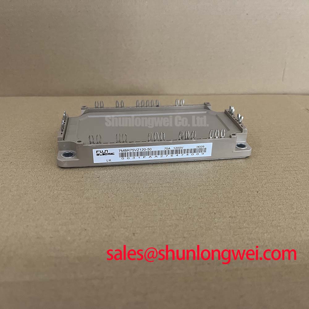
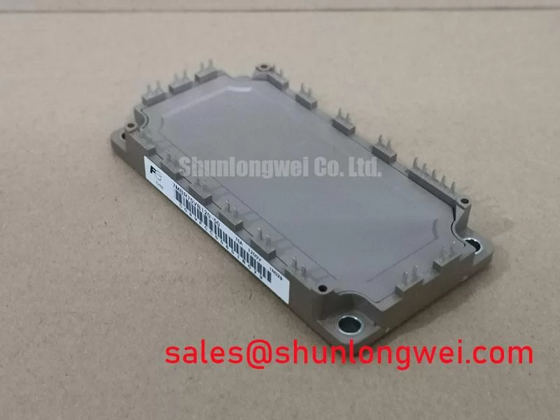
Before energizing a repaired power stage, verify the module marking against the drive documentation and check the disconnected power terminals for an abnormal low-resistance path. The 7MBR75SA120-50 has a specified 1200 V voltage rating and a rated 75 A current under specified conditions in a module package.
| Parameter | Specification |
|---|---|
| Manufacturer | Fuji Electric |
| Part number | 7MBR75SA120-50 |
| Voltage rating | 1200 V |
| Current rating | 75 A under specified conditions |
| Product category | PIM power module |
| Package | Module |
For product family context, Fuji Electric publishes information on power semiconductor and IPM modules and its PIM 7 Pack range. The original equipment schematic and module documentation remain the controlling references for terminal assignment, driver interface, protection thresholds, and switching conditions.
When replacing a 7MBR75SA120-50 module, inspect the heatsink land for raised burrs, corrosion residue, old hardened interface compound, or local distortion before fitting the new module. Uneven contact can create a localized thermal path problem that is difficult to distinguish from a gate drive or load fault during early commissioning.
As a Design Consideration, thermal interface material should be applied as a controlled thin and continuous layer. In many power module assemblies, a nominal interface thickness in the 50 to 100 μm range is used as an assembly reference, but the correct material, coverage, clamping method, and final thickness must be determined from the heatsink design and the applicable module documentation. Use a sequential fastening pattern so contact pressure develops evenly across the baseplate rather than loading one area first.
🔧 Bench Diagnostic: De-energize the DC link and confirm stored energy is discharged before removing gate or power connections for measurement.
After installation, compare switching waveforms with a known stable channel under equivalent loading. Turn-off overshoot, ringing frequency, and current transition shape can indicate an issue in the busbar loop, gate return path, interface contact, or measurement setup. This is an Engineering Recommendation, not an electrical performance guarantee for this specific module. Keep the power loop physically compact and use the original driver return routing to reduce parasitic inductance during turn-off tests.
Field Diagnostics and Commissioning: Isolation Barrier Checks in 7MBR75SA120-50 Topologies
The 1200 V rating defines an official device voltage boundary, but it does not establish the isolation rating of an inverter cabinet, gate driver supply, current sensor, cable harness, or control interface. During commissioning, engineers should verify reinforced galvanic isolation requirements at the system level against the applicable equipment standard and the actual driver data. A specified isolation withstand value or common-mode transient immunity value must not be assumed from the module part number.
Complementary switching commands require an interlock path that remains effective during controller reset, supply ramping, fault handling, and gate-driver desaturation events. Dead time is a system-determined setting: it must cover the actual turn-off behavior, propagation variation, diode commutation, temperature range, and observed waveform timing without creating unnecessary output distortion. If unintended gate activity appears during a switching transition, inspect the gate-to-emitter measurement reference, driver supply stability, controller timing, and common-mode coupling before attributing the event to the power module.
Where the original inverter architecture provides separate power and signal return paths, preserve that arrangement during service. If the original documentation identifies an auxiliary emitter or low-inductance gate return connection, route it only as specified by the equipment design. Combining sensitive gate returns with high-current power returns can obscure commissioning results and increase susceptibility to switching noise.
7MBR75SA120-50 Operational Boundaries: Evaluating Output Filters and Cable Reflection
Long motor leads can behave as transmission lines rather than simple conductors. A mismatch between cable impedance and motor impedance can reflect a switching edge back toward the inverter, producing a motor-terminal peak that is materially higher than the local DC-link expectation. This is a system behavior, not an Official Specification of the 7MBR75SA120-50.
For inverter welder or medium-frequency induction-heating equipment, confirm the output path actually present in the machine before changing a reactor, cable, or filter. Capture voltage at the inverter output and near the load with a measurement arrangement suitable for the expected common-mode environment. Compare the results with the equipment voltage limits, insulation system requirements, and the 1200 V module rating. A dv/dt reactor or sinusoidal filter should be evaluated where cable length, edge rate, load construction, and measured reflection indicate a need, with final selection validated in the finished system.
Engineers assessing a lower-current family member can review the 7MBR35UA120 as a separate part reference. Its suitability cannot be concluded from a current rating alone. Circuit topology, loading profile, cooling arrangement, package interface, protection implementation, and original equipment requirements all require comparison.
For broader context when evaluating switching margin, layout discipline, and emerging wide-bandgap approaches, see Wide Bandgap Revolution. Any comparison must remain tied to measured system voltage, current, thermal, and transient conditions.
Preventing Spurious Faults: Dynamic Gate Impedance Control for 7MBR75SA120-50
High switching dv/dt can couple through gate capacitance and wiring inductance, potentially disturbing the commanded off state of the complementary device. Dynamic gate impedance control is therefore a Design Consideration for the complete driver and module assembly. A dedicated active Miller clamp, where supported by the original driver architecture, can provide a low-impedance off-state path once the gate voltage reaches the clamp operating region. Its behavior must be verified against the driver documentation and measured switching waveforms.
Negative gate bias is also a driver system decision rather than a published requirement for this module. The selected off-state bias must be compatible with the gate driver, isolation barrier, protection circuit, module documentation, and measured transient environment. Engineers should check that the driver remains within its own supply and output limits throughout startup, switching, shutdown, and fault recovery.
When parallel power paths are present, do not assume static or dynamic current sharing from general semiconductor temperature behavior. Measure current distribution and switching timing under representative thermal conditions. Review gate resistor placement, driver path symmetry, busbar geometry, and freewheel commutation behavior together, because a change in one path can alter both switching stress and noise coupling elsewhere in the inverter.