

Content last revised on October 3, 2026
BSM75GP120 Identification and Ratings
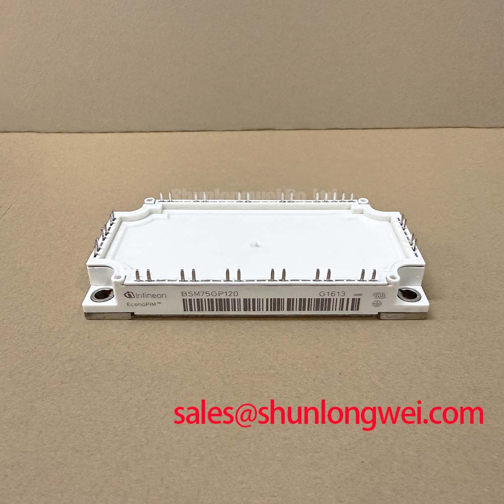
Before installation, isolate the inverter or power supply, inspect the module body and terminals, and verify the nameplate boundary against the replacement record: BSM75GP120 is an Infineon IGBT Module specified at 1200.0 V and 75.0 A. The available factory data identifies the package as a module; gate pin assignment, switching characteristics, thermal resistance, surge capability, and internal topology should be confirmed from the applicable Infineon documentation before commissioning.
| Parameter | Official Specification |
|---|---|
| Manufacturer | Infineon |
| Model | BSM75GP120 |
| Product category | IGBT Module |
| Rated voltage | 1200.0 V |
| Rated current | 75.0 A |
| Package | Module |
These values establish the primary identification and rating reference for equipment repair. They do not, by themselves, establish a permitted operating point for every inverter welder or medium-frequency induction heating supply. The system designer should verify switching frequency, duty cycle, cooling conditions, pulse current, short-circuit protection, gate-drive compatibility, and the original circuit topology before approving a replacement.
Infineon’s official IGBT portfolio provides the appropriate manufacturer-level context for power semiconductor families. As a distributor, we recommend treating the original equipment documentation and the applicable device datasheet as the controlling references for final qualification.
Benchtop Waveform Tuning: Voltage Margin and Environmental Stress Assessment
For a benchtop repair, begin with a controlled no-load inspection of the DC link, gate-drive supply, and switching-node waveform. Confirm that the gate command reaches the intended device terminals with clean turn-on and turn-off transitions, then compare the repaired phase or chopper leg with a known-good channel. A differential high-voltage probe and an isolated measurement arrangement are appropriate for observing collector-emitter overshoot without introducing an unintended measurement path.
The 1200.0 V rating is an official device specification, not a recommended DC-bus operating voltage. During turn-off, stray inductance and current transition rate can raise the instantaneous collector-emitter voltage above the static bus level. The practical design objective is to keep measured switching peaks within the complete system’s verified voltage margin, using the snubber, bus structure, gate resistance, and switching profile selected by the equipment designer.
Cosmic-ray and terrestrial-neutron effects can be relevant in high-voltage semiconductor reliability discussions, particularly when equipment is operated at elevated locations. No SEB FIT rate, altitude derating curve, or cosmic-ray robustness value is provided in the supplied product data for this model. It would therefore be inappropriate to assign a failure probability or claim a specific altitude limit. For installations above the original equipment’s validated environmental range, engineers should perform a documented voltage-margin review and obtain applicable manufacturer reliability information before changing the operating envelope.
On the bench, monitor the DC-link voltage during regenerative events, startup, and abrupt load removal. If an unexpected trip occurs, record the bus waveform, gate-emitter waveform, driver supply behavior, and fault timing together rather than attributing the event to the IGBT alone. A gate signal that appears correct at the driver output may still be distorted at the module terminals by common-emitter inductance, connector impedance, or an interrupted return path.
The Power Electronics Masterclass can be used as a practical reference when reviewing voltage headroom, switching stress, and system-level IGBT selection. It should supplement, not replace, the applicable Infineon documentation and the original equipment manufacturer’s test limits.
Field Diagnostics and Braking-Chopper Commissioning
In an industrial inverter welder or medium-frequency induction heating supply, the braking or chopper path may be responsible for absorbing energy that would otherwise raise the DC-link voltage. The correct selection of the external braking resistor depends on the machine’s stored mechanical or electromagnetic energy, repetition rate, allowable bus rise, cooling method, and control strategy. The 75.0 A rating of BSM75GP120 is an official headline rating and should not be converted directly into a resistor power rating without the device’s complete pulse, thermal, and switching data.
During commissioning, check whether the chopper command is synchronized with the DC-link measurement and whether the resistor is physically capable of dissipating the required pulse energy. Inspect the resistor connections for heat discoloration, looseness, and insulation tracking. A resistor that measures correctly when cold may still be unsuitable under repeated deceleration or high-frequency heating duty because its thermal response and pulse-energy capability are system-dependent.
Fast semiconductor fuse coordination requires a comparison between the fuse clearing characteristic, the prospective fault current, the circuit stray inductance, and the IGBT’s permitted short-circuit or surge behavior. The fuse I²t value should be evaluated against the complete protection sequence, including detection delay and gate turn-off time. The module’s basic voltage and current identification does not provide enough information to declare a suitable fuse or a guaranteed dead-short protection interval.
When a repaired power stage trips immediately, isolate the gate driver from the power circuit where the equipment procedure permits, then check the driver supply, gate return continuity, fault latch, and desaturation or overcurrent feedback path. An abnormal result may arise from a driver fault, a current-sensor problem, a damaged clamp network, or an installation error. Oscilloscope comparison with an undamaged channel is more reliable than assigning one symptom to one component.
For procurement teams reviewing a compatible repair option, the BSM75GD120DLC may be evaluated as a separate device option, but mechanical fit, electrical ratings, pin arrangement, switching behavior, and control-board compatibility must be checked independently. It should not be treated as an automatic substitute for BSM75GP120.
Baseplate Thermal Interface Control During Replacement
Thermal preparation often determines whether a replacement module survives its first production cycle. Remove the old thermal interface material completely, clean the heat-spreader surface using an approved process, and inspect the baseplate and heatsink for burrs, contamination, corrosion, or visible distortion. The interface compound should be selected for the clamping method, operating temperature, electrical insulation requirements, and long-term pump-out behavior documented by its supplier.
The thermal compound must form a continuous interface without excessive voids, but the final layer should be governed by the compound manufacturer’s application instructions and the actual surface condition. Excess material can migrate toward insulation surfaces, while insufficient material can leave dry regions and increase contact temperature. Do not infer a fixed grease thickness from the module’s 1200 V or 75 A rating; interface thickness is an assembly variable requiring process control.
Install the module on a clean, correctly aligned heatsink and tighten the mounting hardware using the equipment or module manufacturer’s specified sequence and torque. A staged, diagonal sequence helps distribute contact pressure across the baseplate. After assembly, inspect for rocking, uneven seating, displaced compound, or evidence that the fasteners have bottomed before the baseplate is clamped.
Maintenance Note: Record heatsink cleanliness, fan or airflow condition, terminal tightness, and measured contact temperature during scheduled maintenance so that gradual thermal deterioration is visible before an overload trip.
At commissioning, measure temperature at comparable load points and compare the repaired leg with the remaining phases. A higher temperature may involve airflow imbalance, thermal interface variation, current sharing, switching loss, or an inaccurate sensor. Thermal conclusions should be based on stabilized measurements and the equipment’s permitted temperature limits rather than on the package label alone.
Busbar Geometry and Gate-Loop Control for Stable Switching
Use a compact, symmetrical power path when connecting the module into a high-current inverter or induction-heating converter. Keep the forward and return conductors closely coupled, minimize unnecessary loop area, and place the DC-link film capacitance according to the original commutation path. The purpose is to reduce parasitic inductance that can convert a rapid current transition into collector-emitter overshoot and ringing.
The switching peak can be understood through the relationship between DC-link voltage, parasitic inductance, and current transition rate: as either inductance or transition rate increases, the transient voltage contribution increases. The acceptable clamp level must be established from measured waveforms and the system’s verified voltage margin. A 25 nH target is not an official BSM75GP120 specification and should not be presented as a universal installation limit; the final busbar geometry must be validated by the equipment engineer with the intended current and switching conditions.
Snubber selection is similarly system-determined. Engineers should evaluate the measured ringing frequency, switching energy, capacitor voltage rating, resistor pulse capability, and thermal dissipation before selecting component values. A snubber that suppresses one operating point can add loss or alter turn-off behavior at another. Verify the result with a properly rated probe during startup, full load, regenerative operation, and fault-recovery testing.
Gate-loop layout deserves the same attention as the power loop. Keep the drive path and return path tightly coupled, avoid sharing high-current emitter paths with sensitive control references, and verify the gate waveform directly at the module terminals. If ringing is present, an engineering recommendation is to adjust damping only after measuring the cause; changing gate resistance without checking driver output impedance, isolation capacitance, and common-mode transient behavior can produce slower switching without resolving the underlying fault.
For an isolated industrial drive board, verify the selected optocoupler or digital isolator’s common-mode transient performance against the actual switching waveform. The isolation component, gate driver, protection latch, and DC-link sensing circuit must operate as one coordinated protection chain. Test desaturation or overcurrent soft turn-off under controlled conditions, confirm that the fault signal reaches the controller, and verify that the gate is held inactive after a fault until the intended reset sequence is completed.