
Content last revised on November 7, 2026
MG75Q2YS40 Circuit Protection & Reliability: Calibrating Ceramic Substrate Mounting Integrity
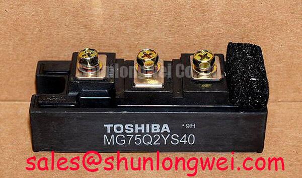
Manufacturer: Toshiba | Part Number: MG75Q2YS40 | Class: IGBT Module | Key Rating: 1200.0 V, 75.0 A
When a repaired drive shows unstable thermal behavior, inspect the copper baseplate convexity and heatsink flatness before changing the power stage. A local high spot can reduce the effective thermal interface area, while uneven clamping can stress the ceramic substrate and create a mechanical fault that appears only after thermal cycling.
The MG75Q2YS40 is a Toshiba IGBT Module with a Collector-Emitter Voltage (Vces) rating of 1200.0 V and a Continuous Collector Current (Ic) rating of 75.0 A under the specified datasheet conditions. Its specified Package is Toshiba Module, and its Configuration / Topology is IGBT Power Stage. The circuit arrangement is identified as a Half-Bridge Dual IGBT structure, so the mounting surface and busbar alignment should be treated as part of the switching circuit rather than as a separate mechanical detail.
As a Design Consideration, clean both mating surfaces with a process approved for the heatsink and interface material, then check flatness with an appropriate inspection method. The thermal interface material should form a continuous, thin layer without dry islands, trapped particles, or excess material pushed toward the terminals. A commonly used engineering reference for this type of assembly is a controlled TIM layer in the approximate 50–80 µm range, but the final thickness depends on the selected material, surface finish, and supplier instructions.
Use a diagonal cross-pattern tightening sequence so the module seats progressively instead of tilting against one corner. A torque-controlled tool is preferable to hand estimation, and the final value must follow the module fastening specification, heatsink hardware, and interface material requirements. 💡 Pro Tip: Do not tighten one mounting point fully before the others, because local loading can distort the contact pattern and place unnecessary stress on the substrate.
During field diagnosis, compare the thermal contact imprint after removal with the expected footprint. A narrow imprint, an untouched region, or excessive squeeze-out can indicate a flatness, alignment, or fastening issue. Designers integrating this device into an electric forklift traction inverter should also preserve clearance around the high-voltage terminals and prevent the heatsink, busbar, or fasteners from becoming unintended current paths.
MG75Q2YS40 Circuit Protection & Reliability: Calibrating Long-Motor-Lead Voltage Spikes
Long motor cables behave as transmission lines at fast switching edges, so a traction inverter can experience reflected-wave overshoot at the motor terminals even when the DC link appears well controlled. A measured spike approaching twice the local DC voltage should be treated as a system interaction involving cable impedance, motor impedance, switching speed, termination behavior, and physical routing.
The practical investigation starts at the inverter output and then moves to the motor terminals using a correctly rated differential probe. Compare the waveform with short and extended cable configurations, and inspect whether the ringing frequency or peak level changes with cable routing. This helps distinguish a transmission-line effect from a commutation-loop problem inside the inverter.
Filtering and choke selection should be based on the complete motor-cable network. An output filter can reduce edge energy, but it also changes common-mode current, control response, and the voltage stress seen by the switching devices. The system designer should select the filter after reviewing motor insulation limits, cable construction, switching frequency, and the measured terminal waveform. The 1200.0 V Vces rating of the MG75Q2YS40 is an official device rating, not a substitute for verifying transient voltage margin in the assembled drive.
Short-circuit protection requires a coordinated gate-driver response. A desaturation circuit can monitor the rising collector-emitter voltage while the IGBT is commanded on and initiate a controlled shutdown, while a two-stage soft turn-off sequence can limit the rate of current interruption during a fault. A sub-3 µs response may be used as an engineering design target in some drive architectures, but the actual blanking interval, detection delay, gate resistance, and soft turn-off profile must be established from the driver, power loop, and short-circuit test results.
For gate-drive reference material, engineers can review ROHM dedicated gate driver ICs for IGBT and SiC applications. The driver interface should be validated for dead-time coordination, fault reset behavior, isolation, and the possibility of Miller-induced turn-on during the opposite switch transition.
MG75Q2YS40 Circuit Protection & Reliability: Calibrating Braking Energy and Overvoltage Trips
Regenerative braking can raise the DC-link voltage when the traction motor decelerates faster than the battery or front-end converter can absorb energy. If a resistive braking path is required, its IGBT and braking resistor should be selected from the vehicle mass, speed, wheel radius, gear ratio, deceleration profile, duty cycle, DC-link capacitance, and allowable battery charging conditions.
The MG75Q2YS40 may be evaluated within a braking topology when its voltage, current, switching, thermal, and short-circuit requirements match the system design. The official ratings of 1200.0 V Vces and 75.0 A Ic under the specified datasheet conditions provide the primary device identification, while braking resistor energy and pulse loading remain system-level calculations. The resistor must tolerate the expected pulse energy and repetition pattern without creating a thermal hazard inside the enclosure.
Fast switching improves response but increases sensitivity to wiring inductance, gate-loop coupling, and voltage overshoot. Place the braking switch and its local energy path so that the high-current loop remains compact and mechanically supported. A snubber or clamp network can be considered when oscilloscope measurements show excessive ringing, but its capacitance, damping, voltage rating, and dissipation must be selected from the measured waveform rather than copied from an unrelated inverter.
When a drive reports repeated overvoltage trips, capture the DC-link waveform during acceleration and deceleration, then compare the event with the braking command and resistor temperature. Check the gate signal at the module terminals rather than only at the driver output. A missing pulse, delayed turn-on, or incomplete turn-off can point toward driver supply behavior, isolation timing, gate-loop impedance, or control sequencing rather than the power module alone.
For a cross-reference review, the MG100Q2YS51 is a separate Toshiba module entry that may be assessed objectively when a different current class or package requirement is present. Any substitution requires a complete comparison of electrical ratings, gate-drive conditions, mechanical fit, thermal impedance, protection behavior, and control firmware limits.
Preventing Spurious Faults: High-Frequency Commutation Loop Inductance Guidelines for MG75Q2YS40
Keep the high-frequency commutation loop compact and geometrically balanced to reduce turn-off overshoot and false protection events. The relevant loop includes the DC-link capacitor, upper and lower switching paths, module terminals, and the return conductor. Wide conductors alone are not sufficient if the outgoing and return paths are separated by a large area.
The peak voltage contribution from stray inductance rises with both loop inductance and current slew rate; in practical terms, the assembled circuit follows the relationship in which peak voltage is the DC-link voltage plus the inductive term associated with current change. The engineering task is to minimize that parasitic loop and verify the resulting peak against the MG75Q2YS40 voltage rating during switching tests.
A symmetrical planar busbar can reduce magnetic loop area and help keep the upper and lower commutation paths predictable. The final geometry, spacing, insulation system, and clearance must be coordinated with the enclosure, creepage requirements, service access, and production tolerances. A value such as 25 nH may appear in a particular converter design target, but it is not an official MG75Q2YS40 specification and should not be treated as a universal installation limit.
Snubber capacitors, RC damping networks, or active clamp circuits can be evaluated when the measured waveform contains a narrow high-frequency spike or sustained ringing. Probe grounding is critical: a long probe lead can create an artificial oscillation and lead to incorrect component selection. Use a suitable differential measurement method at the module terminals and correlate the power-switching waveform with the gate-emitter waveform measured at the module.
Gate-loop routing should remain separate from the power commutation path, with a short return to the driver reference and controlled coupling to the opposite switch. Designers should verify dead time under temperature and load variation so that the half-bridge does not enter cross-conduction during transitions. For thermal and transient design guidance related to power conversion systems, see Preventing Derating and Maximizing EV Performance.