


Content last revised on September 10, 2026
Incoming Quality Control & Parametric Baseline: Infineon FZ800R16KF4
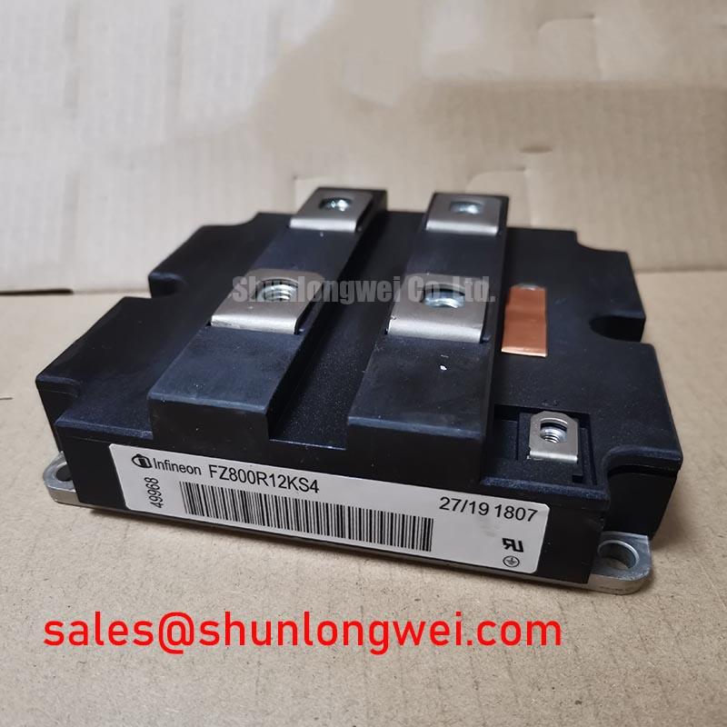
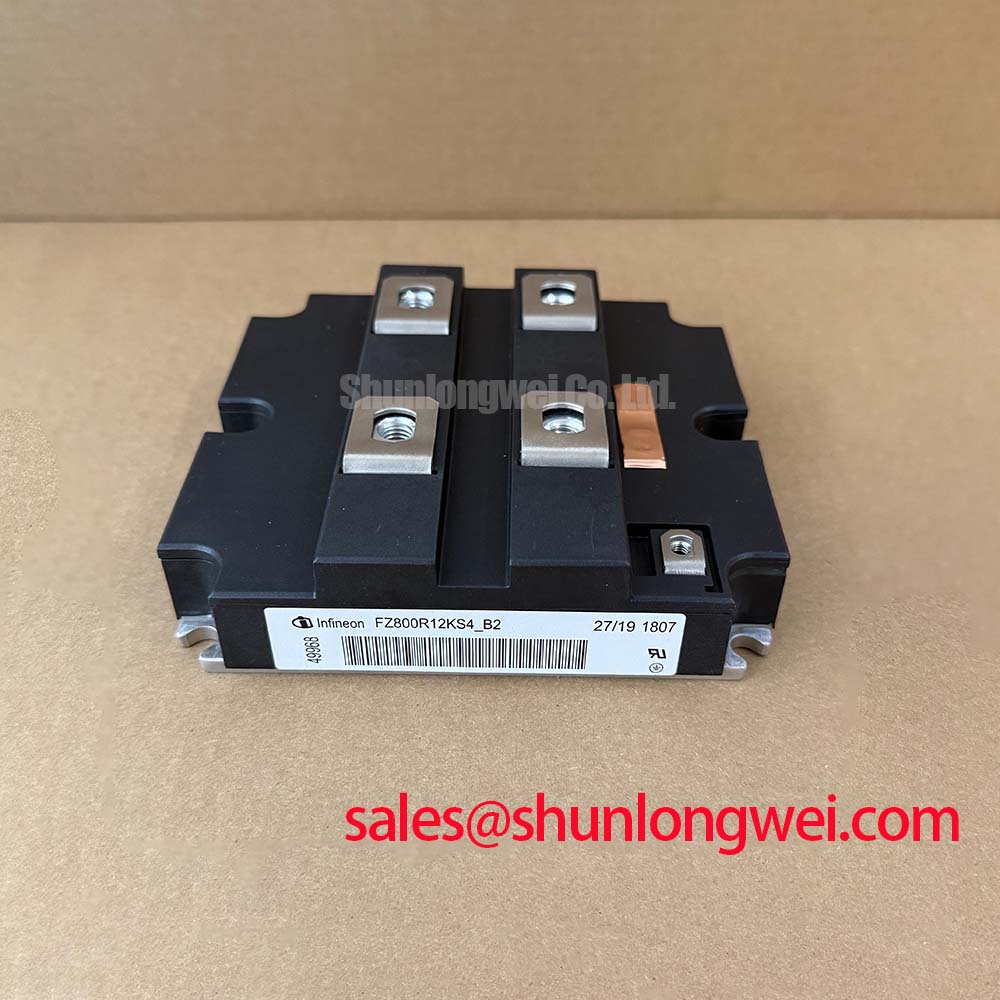
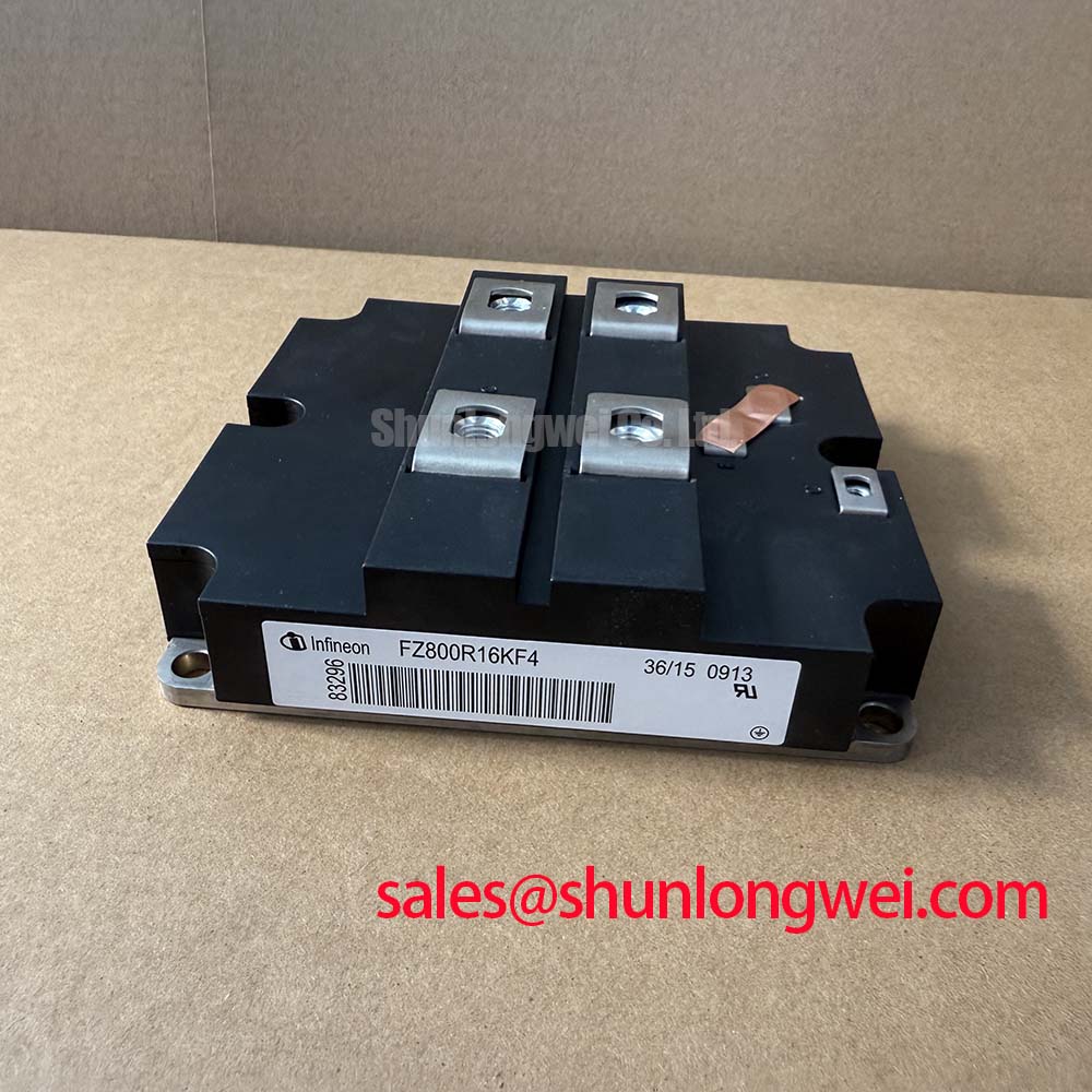
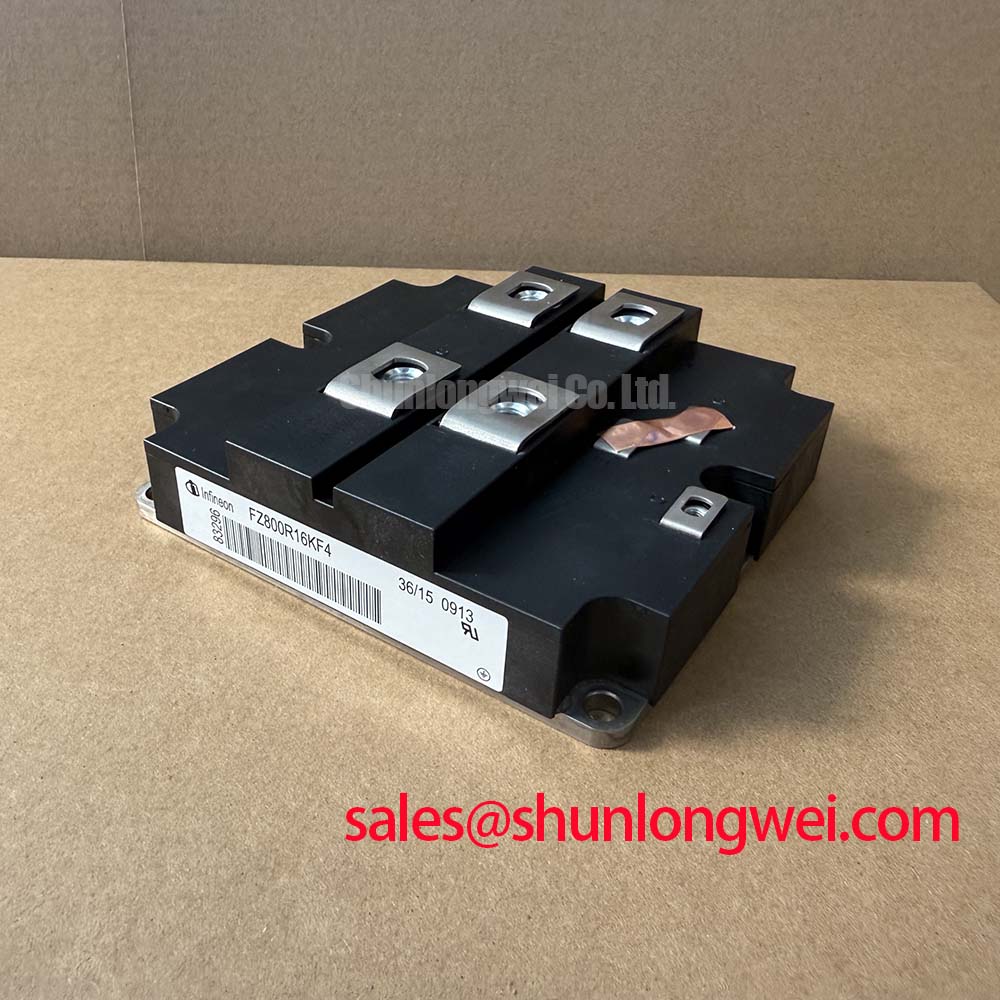
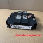
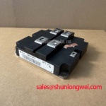
In power semiconductor receiving inspection, validating electrical parameters before mechanical integration prevents field downtime in utility-scale installations. The FZ800R16KF4 is a single-switch IGBT module housed in an industry-standard 130mm x 140mm footprint with an isolated copper baseplate. When unpacking lots in the incoming test bay, the initial protocol requires verification of static gate threshold behavior, terminal isolation, and freewheeling diode characteristics across a calibrated test fixture.
| Parameter | Symbol | Specification Value | Test Conditions | Data Classification |
|---|---|---|---|---|
| Collector-Emitter Voltage | VCES | 1600 V | Tvj = 25°C | Official Datasheet Specification |
| Continuous Collector Current | IC,nom | 800 A | TC = 80°C | Official Datasheet Specification |
| Repetitive Peak Collector Current | ICRM | 1600 A | tp = 1 ms | Official Datasheet Specification |
| Collector-Emitter Saturation Voltage | VCE(sat) | 2.40 V (typ.) / 3.00 V (max.) | IC = 800 A, VGE = 15 V, Tvj = 25°C | Official Datasheet Specification |
| Gate-Emitter Threshold Voltage | VGE(th) | 5.0 V (min.) – 6.5 V (max.) | IC = 32.0 mA, VCE = VGE, Tvj = 25°C | Official Datasheet Specification |
| Thermal Resistance (Junction-to-Case) | Rth(j-c) | 0.024 K/W (max. per IGBT) | Single IGBT element | Official Datasheet Specification |
| Short Circuit Withstand Time | tpsc | 10 µs | VGE ≤ 15 V, VCC = 900 V, Tvj op ≤ 125°C | Official Datasheet Specification |
| Operating Junction Temperature | Tvj op | -40°C to +125°C | Continuous continuous switching window | Official Datasheet Specification |
💡 Bench Tip: Prior to unshorting the auxiliary control terminals, clip an ESD wrist strap directly to the ground point of your curve tracer. Never touch gate pins with bare hands. For cold-state diode screening, run a constant forward current of 10 A across the antiparallel diode terminals at 25°C; an intact silicon junction typically exhibits a forward voltage drop between 0.85 V and 1.15 V (Bench Screening Baseline). Readings outside this window or open-circuit indications immediately flag damaged internal bond wires or lattice defects.
DC-Bus Operating Voltage Headroom Derating for Single Event Burnout (SEB) Immunity
Operating high-capacity central solar inverters at 1500 V DC nominal presents severe vulnerability to terrestrial neutron radiation. Atmospheric neutrons generated by cosmic ray cascades can trigger Single Event Burnout (SEB) inside high-voltage planar and trench junctions. Although rated for VCES = 1600 V (Official Datasheet Specification), running the FZ800R16KF4 at prolonged sustained voltages above 1000 V at elevations above 2000 meters significantly escalates the cumulative Failure in Time (FIT) rate.
Engineering evaluations must establish strict DC-bus headroom derating based on standards defined by the JEDEC Solid State Technology Association Standards (such as JESD89A for terrestrial neutron testing). When deployed at high altitudes, the cosmic neutron flux density multiplies exponentially compared to sea-level environments. To secure continuous 25-year reliability targets in utility solar farms, the operating bus voltage per module is typically restricted below 950 V to 1000 V (Design Consideration for terrestrial cosmic ray mitigation). For systems demanding higher blocking margin under two-level or multi-level schemes, engineers often evaluate higher-voltage platforms, such as the related FZ1000R33HE3 module rated at 3300 V.
Field troubleshooting across remote inverter cabins should always include altitude-adjusted leakage current evaluations. In our QA screening, applying a steady 1280 V across the collector-emitter terminals (80% of nominal VCES) at 25°C must yield an off-state leakage current ICES well below 5.0 mA (Official Datasheet Specification limit). A sudden deviation indicates localized crystal degradation or compromised passivation layers along the chip periphery.
Transient Thermal Impedance (Z_th(j-c)) & Multi-Layer Foster/Cauer Modeling
Utility-scale central inverters operate under dynamic thermal cycling driven by passing clouds, grid faults, and active reactive power tracking. The internal junction temperature rises rapidly during sudden insolation bursts. Modeling these thermal transients requires analyzing the thermal impedance Zth(j-c) across multi-stage Foster and Cauer ladder networks, tracking heat transfer through silicon dies, solder interfaces, direct bonded copper (DBC) ceramic substrates, and the heavy copper baseplate.
The steady-state junction-to-case thermal resistance Rth(j-c) is specified at a maximum of 0.024 K/W per IGBT (Official Datasheet Specification). When absorbing short-duration overloads, transient thermal capacitance delays heat propagation to the heatsink. Under surge conditions, total parasitic loop inductance in the external DC bus must be constrained below 25 nH (Design Consideration) through low-inductance laminated busbars and high-frequency snubber film capacitors mounted directly across terminals 1 and 2. Excessive busbar inductance induces severe di/dt transient overvoltage spikes during IGBT turn-off that easily breach the 1600 V collector breakdown threshold. For deep-dive test procedures on dynamic pulse thermal response and power cycling validation, consult the Field Engineer’s Handbook for established test criteria.
⚠️ Field Alert: Substrate flatness and thermal interface material (TIM) thickness are critical failure points. Never apply thermal paste thicker than 100 µm; an optimal layer measures between 50 µm and 80 µm (Design Consideration). Torque the M6 baseplate mounting bolts in a diagonal, two-stage cross pattern: first hand-tighten to 2.0 N·m, then ramp sequentially to the final specification of 3.0 to 6.0 N·m (Official Datasheet Specification). Uneven torquing bows the internal ceramic substrate, resulting in micro-cracking and localized thermal runaway under heavy load cycles.
Common-Mode Transient Immunity (CMTI > 100kV/us) in Harsh Industrial Environments
High-current, medium-voltage power stacks subject gate drive interfaces to high dv/dt transients exceeding 15 kV/µs during rapid IGBT turn-off. In central PV arrays, common-mode ground noise couples directly into low-voltage gate drive circuitry via inter-winding capacitance of auxiliary DC-DC transformers and isolated optocouplers. Gate drive topologies interfacing with the FZ800R16KF4 require Common-Mode Transient Immunity (CMTI) rated at 100 kV/µs or greater (Design Consideration) to prevent spurious turn-on events.
Spurious gate triggering under high dv/dt occurs when displacement current charges the reverse transfer capacitance (Miller capacitance Cres). If this current generates a voltage drop across the internal and external gate impedance exceeding the lower VGE(th) boundary of 5.0 V (Official Datasheet Specification), parasitic turn-on follows, triggering hazardous DC-bus shoot-through. Implementing an active Miller clamp circuit that short-circuits the gate directly to the negative rail when VGE drops below 2.0 V effectively suppresses these transients.
Dielectric isolation inside high-voltage modules depends on Silicone Gel Encapsulation for High Voltage Insulation to suppress internal partial discharges and resist moisture ingress. During receiving inspection, an insulation test voltage of VISOL = 3.4 kV AC (RMS at 50 Hz for 1 minute, Official Datasheet Specification) applied between the shorted power terminals and the metallic baseplate verifies insulation barrier integrity without dielectric breakdown.
PCB Symmetry Considerations for Dual IGBT Half-Bridge Switching Paths
Paralleling or constructing half-bridge phases with large single-switch modules like the FZ800R16KF4 demands strict geometric and magnetic symmetry in high-current buswork and gate driver PCB routing. Trace length mismatches or asymmetrical loop areas create unbalanced stray inductances, leading to unequal current sharing, localized hot-spotting, and high-frequency ringing.
A primary design rule is separating the auxiliary Kelvin emitter connection from the main power emitter return. The FZ800R16KF4 features dedicated auxiliary control terminals. Routing the gate drive return path through the main emitter conductor introduces the power circuit's high di/dt directly into the gate loop. This inductive voltage drop acts as negative feedback during turn-on and causes oscillation during turn-off. Route gate and auxiliary Kelvin emitter traces as tightly coupled, twisted-pair configurations or adjacent PCB layers to cancel magnetic fields, establishing an initial damping gate resistor RG,ext around 1.8 Ω to 3.3 Ω (Typical Starting Point for bench tuning) to minimize switching oscillations.
In complex multi-stage converter architectures combining central generation with dynamic harmonic filtering, balance and layout discipline extend across intermediate converter tiers. For auxiliary pre-regulators or lower-capacity dynamic brake choppers, engineers routinely pair power blocks with matched half-bridge units, such as the related FZ600R12KE4 dual-switch module. Synchronizing propagation delays across all driver channels within a 20 ns window prevents branch cross-conduction and maintains uniform thermal margins across the entire inverter enclosure.