

Content last revised on October 3, 2026
Initial Identification and Safe Inspection
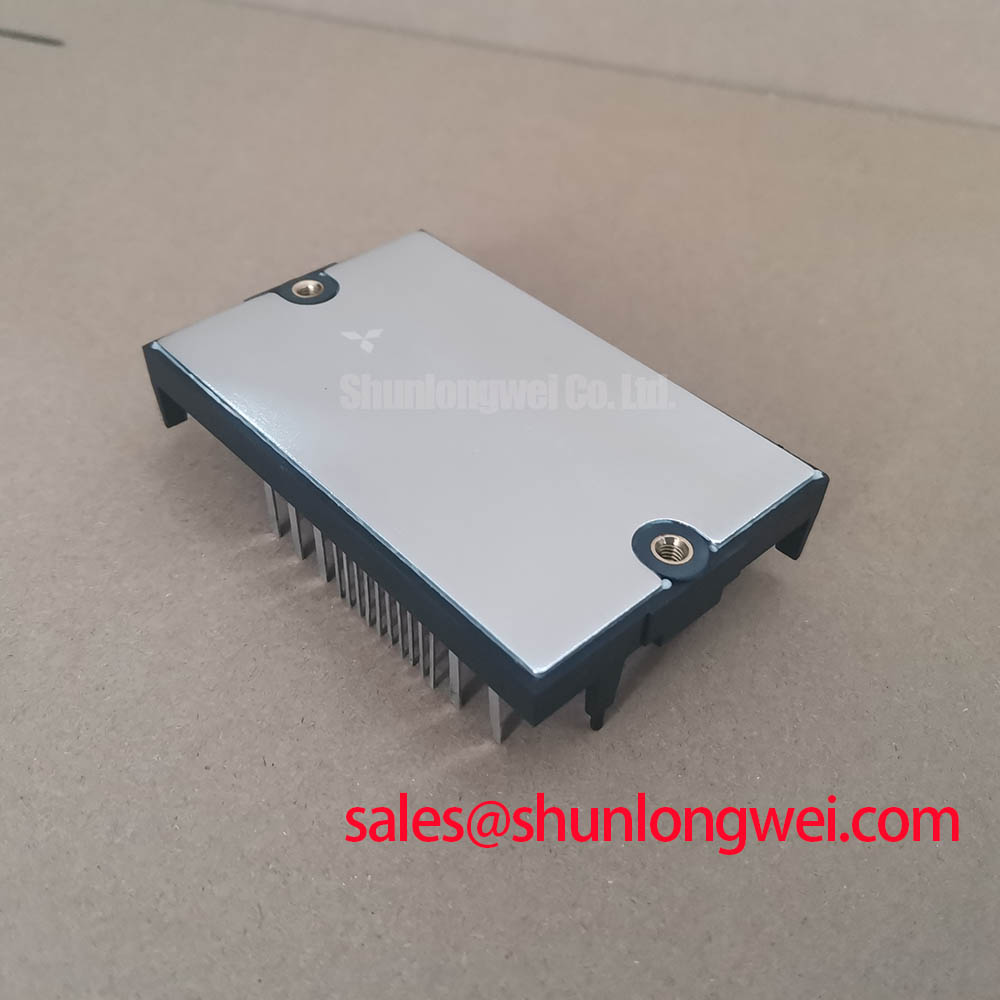
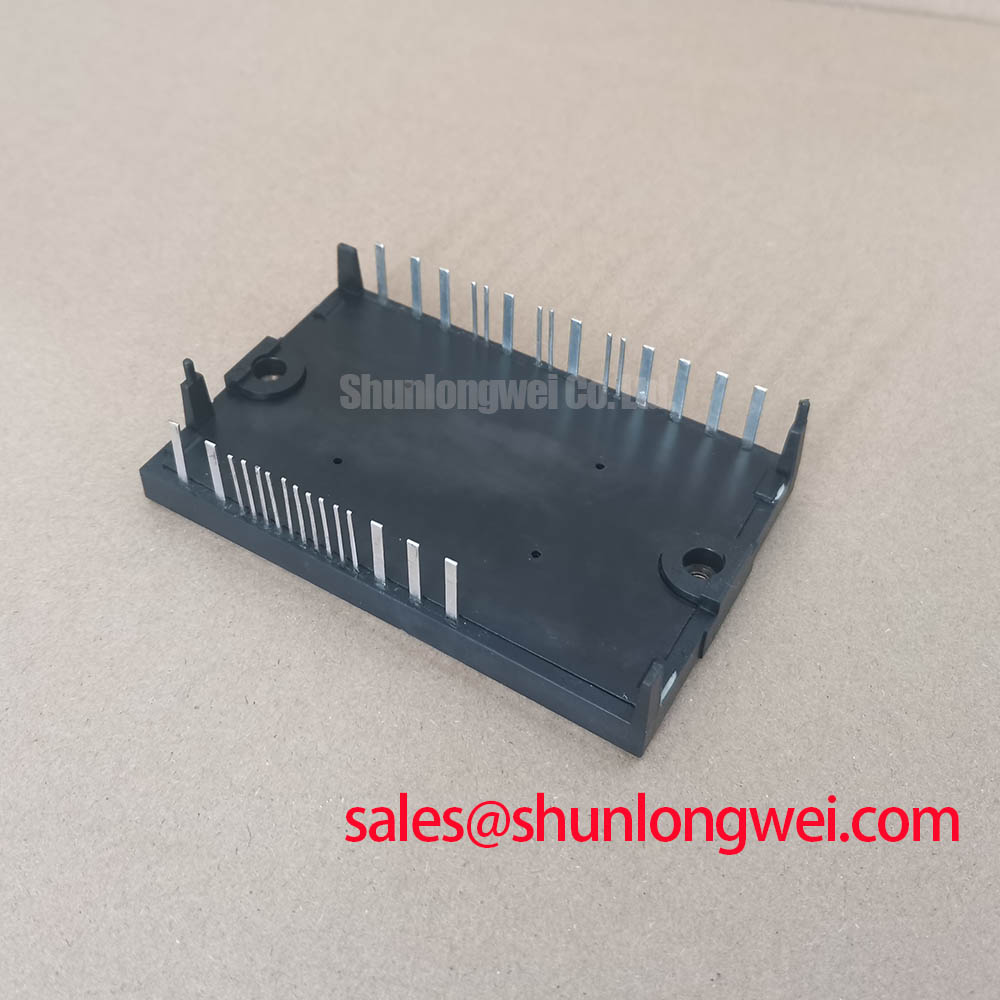
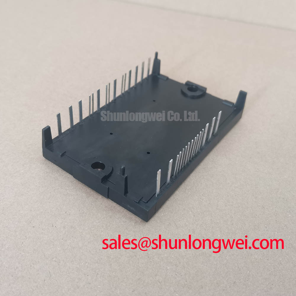
With the DC bus isolated and discharged, perform unpowered resistance or continuity checks at the accessible terminals of the installed J2-Q03A-D against the equipment schematic before removing its connections. Interpret these measurements in view of any parallel circuit paths. Record the terminal positions and inspect the case, fasteners and heatsink contact for visible damage. The supplied product specifications identify this Fuji Electric part as a Power Transistor Module rated at 1600 V and 30 A (Official Specification). Those ratings establish an initial identification check, not a complete compatibility or operating limit assessment.
J2-Q03A-D Electrical Boundaries and Isolation Checks
Trace each J2-Q03A-D terminal to the driver and power circuit before applying a test signal. The module rating alone does not establish its pinout, internal connection, drive requirements or isolation withstand rating. For a replacement assessment, the equipment documentation and the applicable Fuji Electric part drawing should govern those checks. Fuji Electric’s power semiconductor portal is a manufacturer reference for identifying module documentation; its general product pages should not be treated as a substitute for a part-specific drawing.
Design Consideration: If the equipment uses an isolated driver, inspect the driver supply, isolation components and board clearances as a system. An unexpected switching pulse can originate in the driver or its wiring rather than in the power module. Compare suspect waveforms with a known-good channel under controlled test conditions, then verify that switching transients remain within the documented boundaries of the complete assembly. Do not assign a reinforced-insulation or common-mode immunity rating to J2-Q03A-D without a specification that explicitly states it.
Thermal Contact and Mechanical Installation
Before refitting the module, clean the mating surfaces and check the heatsink for raised edges, debris and uneven contact marks. Apply thermal interface material according to the equipment or material supplier’s instructions; the supplied J2-Q03A-D specifications do not state a grease thickness, baseplate flatness limit or mounting torque. Tighten the mounting hardware in the documented sequence so the case seats evenly, and investigate any gap that persists rather than forcing the assembly flat.
Field Alert: Isolate and discharge the DC bus before loosening module terminals or mounting screws.
In an industrial inverter welder or medium-frequency induction heating supply, thermal complaints warrant checks beyond the module: examine cooling flow, terminal condition and the measured load waveform. Design Consideration: If the surrounding circuit includes an RC snubber or phase-angle-controlled input stage, assess those parts against the original schematic; neither function is established as an internal feature of J2-Q03A-D. Fuji Electric’s global power semiconductor information provides manufacturer context, while the equipment service documentation remains the authority for its mechanical installation.
Fault Response and Switching Transients
When a protection trip follows module installation, capture the driver command, sensed fault signal and bus waveform rather than treating the trip as proof of a failed transistor. Check connector seating and the continuity of the sensing path with power removed. During an instrumented restart, compare the suspect channel with an unaffected one where the equipment permits it. The supplied specifications do not establish a J2-Q03A-D short-circuit withstand time, desaturation threshold or soft-turn-off profile, so a driver protection delay cannot be specified from the 1600 V and 30 A ratings alone.
Design Consideration: Keep the switching current path and driver return arrangement consistent with the validated equipment layout to limit inductive overshoot and noise coupling. The system engineer should verify peak voltage and fault response during controlled switching tests against the applicable device and equipment limits. A negative off-state bias or bootstrap supply, if present in the existing driver, must be assessed from that driver’s documentation rather than assumed necessary for this module. For comparison of a different switching technology, The 1200 V CoolSiC™ MOSFET Advantage in Three-Phase Power Conversion discusses SiC MOSFET system considerations; it does not define J2-Q03A-D limits.
J2-Q03A-D Compatibility and DC-Bus Surge Assessment
For an equipment replacement, match the original module’s terminal map, mounting arrangement and documented electrical characteristics before considering a candidate. The listed 7MBR30SA-060-50 can be examined during an alternatives review, but it should not be treated as a direct replacement without comparing the manufacturer documentation and the actual circuit. A shared current figure, where one exists, would not establish voltage, topology or mechanical equivalence.
On a system that experiences DC-bus rise during motor deceleration, determine whether the equipment uses a braking switch and resistor, then inspect that path against its original schematic. Their presence, location and ratings cannot be inferred from the J2-Q03A-D description. Design Consideration: Measure the bus during a controlled deceleration test and have the system designer check the observed peak and resistor duty against documented limits. If the application is instead a welder or induction heater, assess its actual bus transient sources rather than assuming it has a regenerative braking circuit.