



Content last revised on September 27, 2026
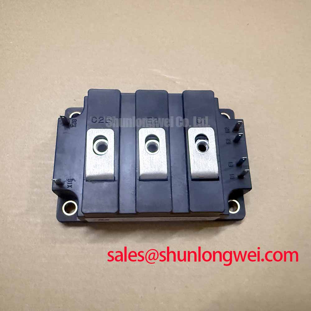
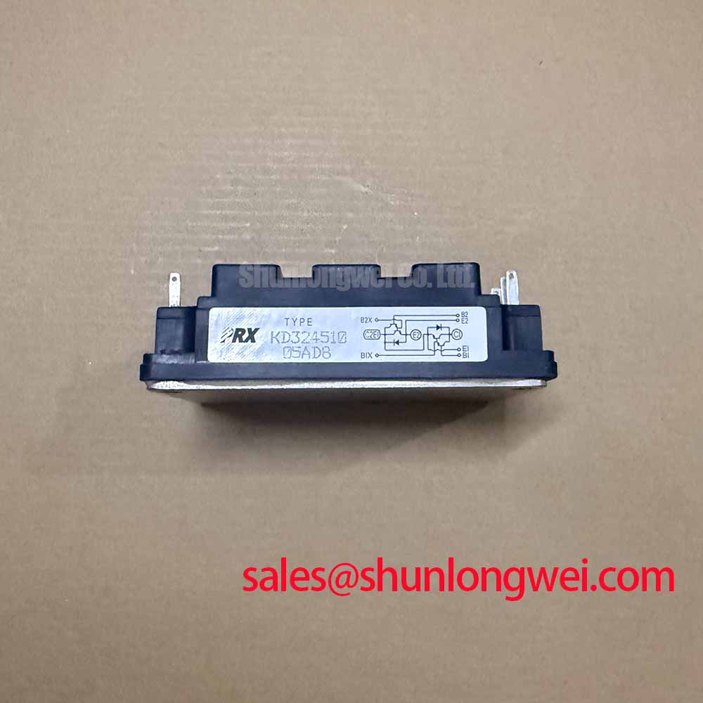
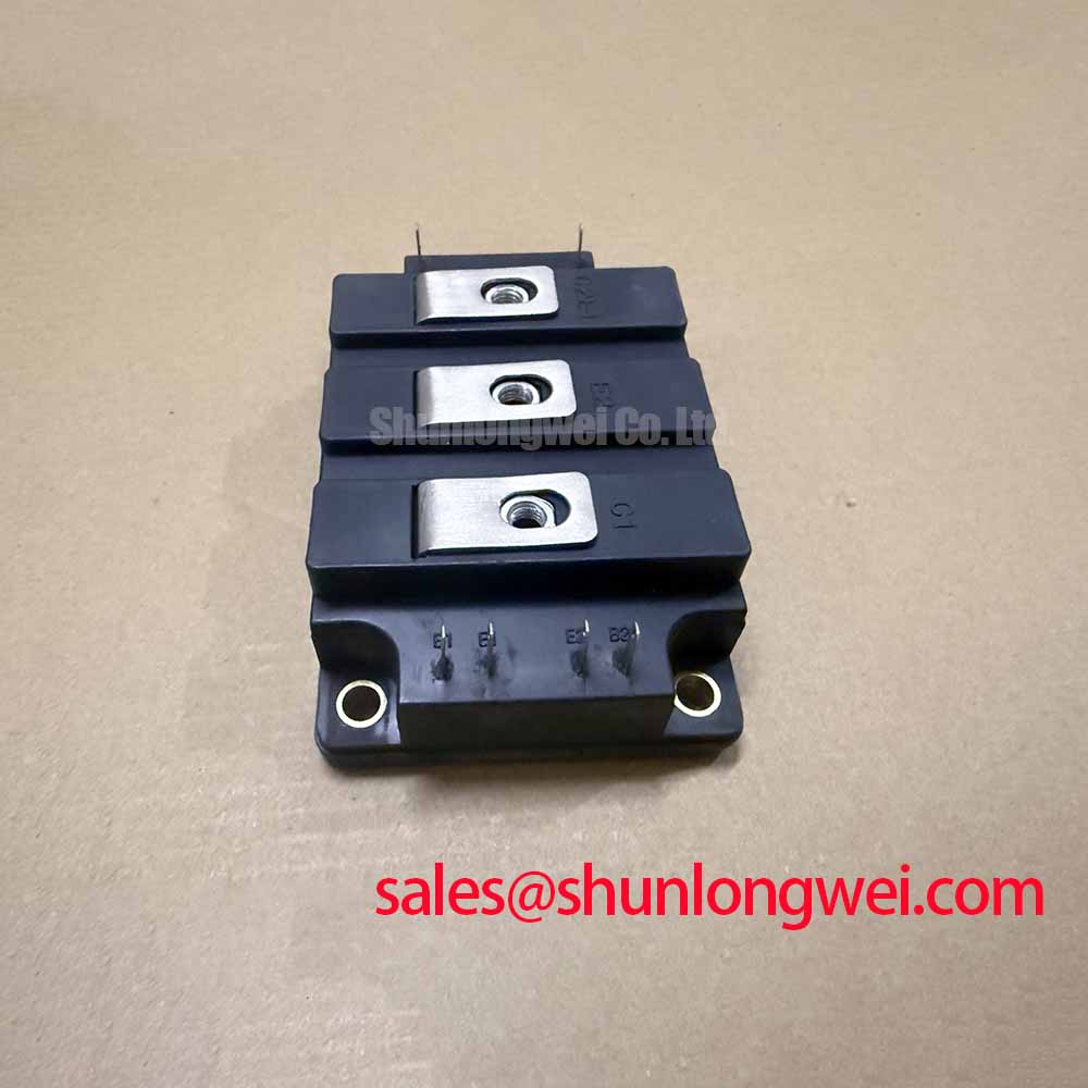
KD324510 SanRex 1000 V 450 A Thyristor Diode Module
With the rectifier isolated and discharged, inspect the KD324510 housing, clean the main terminals, and verify the nameplate against the required 1000 V repetitive peak reverse voltage and 450 A average forward current per circuit under the specified datasheet conditions before removing the original device. A cold resistance check can help identify an obvious short condition, but it cannot reliably establish an open thyristor without appropriate triggering. It is only a preliminary screen and should be compared with a known-good circuit and the manufacturer’s test method.
The SanRex KD324510 is a high-current thyristor and diode module intended for controlled rectifier stages where the switching device, heat path, gate wiring, fuse coordination, and busbar layout must be evaluated as one assembly. Its published electrical data includes a 9000 A maximum surge current for 60 Hz, one cycle, a 1.3 V maximum peak forward voltage drop under the specified test conditions, 0.08 °C/W maximum junction-to-case thermal resistance, and 2500 V RMS isolation voltage under the specified test conditions. These specification values do not replace the ratings of the surrounding converter, fuse, transformer, busbar, or cooling system.
| Parameter | Official specification | Commissioning relevance |
|---|---|---|
| Repetitive peak reverse voltage | VRRM = 1000 V | Verify the applied repetitive reverse voltage and transient margin at the device terminals. |
| Average forward current per circuit | IF(AV) = 450 A under the specified datasheet conditions | Check the actual conduction duty, cooling path, current sharing, and enclosure airflow. |
| Maximum surge current | IFSM = 9000 A, 60 Hz, one cycle | Use for fault and surge coordination review; it is not a continuous operating rating. |
| Maximum peak forward voltage drop | VFM = 1.3 V under the specified test conditions | Review the applicable forward-voltage characteristic and system current waveform when estimating conduction loss. |
| Junction-to-case thermal resistance | Rth(j-c) = 0.08 °C/W maximum | Describes the junction-to-case heat path; the case-to-heatsink interface requires separate assessment. |
| RMS isolation voltage | VISO = 2500 V RMS under the specified test conditions | Verify insulation, creepage, clearance, and test conditions at assembly level; this is not a continuous working-voltage rating. |
Field Diagnostics & Commissioning: Gate Trigger Current Temperature Dependence in KD324510 Topologies
Begin commissioning with the gate and cathode connections de-energized. Confirm terminal identity from the original equipment drawing or the applicable SanRex documentation rather than assuming that a mechanically similar module uses the same control layout. Inspect crimped lugs, busbar contact faces, gate leads, and auxiliary wiring for looseness, discoloration, or mechanical strain. A low-voltage continuity check can identify an open control lead, while a meaningful firing assessment requires the actual gate circuit and an oscilloscope reference at the device terminals.
The product data summarized here does not specify a gate trigger current, gate pulse rise time, holding current, or firing temperature coefficient. Those values must therefore be obtained from the applicable device curve or controlled test documentation before setting a pulse generator or gate driver. When a converter uses repeated firing pulses or a back-porch pulse, the commissioning engineer should verify that the gate waveform remains within the device’s documented limits across cold start, warmed operation, minimum line voltage, and the highest expected load.
Gate wiring should be routed separately from high-current commutation paths where the equipment layout permits. This reduces the opportunity for the power loop to inject unwanted voltage into the firing circuit. The busbar arrangement should also minimize parasitic loop inductance so that turn-off overshoot is controlled during switching transients. The final result must be checked with suitable probing at the module terminals, not inferred from the controller output alone.
Fuse coordination requires the protective device’s published I²t value, clearing time, prospective fault current, and the converter’s transformer impedance, together with the semiconductor’s applicable surge and I²t limits. The KD324510 surge specification of 9000 A for one 60 Hz cycle is a device rating under its stated test condition, not a substitute for a fuse I²t coordination table. If a replacement fuse or gate board is being considered, verify the complete protection chain before energizing the rectifier.
Field Alert: Isolate and discharge the converter before touching gate, cathode, anode, or heatsink connections, and tighten mechanical hardware only according to the equipment manufacturer’s documented assembly procedure.
KD324510 Circuit Protection & Reliability: Calibrating AC-to-DC Transfer Characteristics across Operating Conditions
For a controlled AC-to-DC rectifier, record the line voltage, firing command, load current, DC output, and device temperature during a controlled commissioning sequence. The familiar firing-angle range from 0° to 150° may be useful for system analysis, but it is not a KD324510 product rating. The permitted operating range, pulse timing, commutation method, and load profile are determined by the converter design and must be confirmed from the system documentation.
At lower firing angles, the rectifier may deliver greater average DC output while the line current waveform, transformer utilization, displacement power factor, and reactive power demand change with operating point. At larger firing angles, output regulation and commutation margin require closer review. Measure the actual AC waveform and DC waveform together, especially where a high-current green hydrogen electrolyzer DC power rectifier is being evaluated. A distorted waveform can arise from transformer impedance, commutation overlap, control timing, wiring inductance, or an abnormal device, so a single voltage measurement should not be used to assign a cause.
The KD324510’s 1000 V VRRM rating should be compared with the repetitive reverse voltage at the module terminals, including transient behavior observed during line commutation. The 2500 V RMS isolation specification should be treated separately from the insulation capability of the complete assembly. Enclosure spacing, mounting hardware, contamination, cable routing, and test duration remain system-level responsibilities.
For a replacement assessment, compare the current path, voltage class, mounting geometry, control terminal arrangement, cooling interface, and protection scheme. The SanRex FRS200CA100 can be reviewed as a related device for an objective electrical and mechanical comparison, but substitution requires confirmation of the converter schematic and the applicable device documentation rather than a part-number comparison alone.
In a multi-stage power supply, the upstream rectifier and the controlled output bridge should be reviewed together. The PK55FG120 may be relevant as a complementary stage in some system architectures, subject to its own electrical ratings, topology, and installation requirements. Neither device should be assumed interchangeable without checking the complete circuit.
KD324510 Operational Boundaries: Evaluating RC Snubber Network Optimization to Avoid Exceeding Ratings
An RC snubber should be assessed from measured commutation behavior, not copied from an unrelated converter. Record the voltage across the KD324510 during turn-off and line commutation, identify the peak and ringing frequency, and then evaluate whether the disturbance is associated with busbar inductance, transformer leakage, diode reverse recovery, wiring arrangement, or the snubber itself. The system designer must select resistor and capacitor values after reviewing voltage, current, pulse energy, repetition rate, and component pulse capability.
The KD324510 data summarized here does not specify a recommended snubber resistance, capacitance, allowable dv/dt, reverse-recovery softness factor, or saturable reactor value. These values must not be presented as fixed settings for this module. The practical design principle is to minimize the high di/dt commutation loop and control voltage overshoot while confirming that the snubber does not create excessive reactive current or resistor heating. Oscilloscope measurements should use a properly rated differential probe and a short measurement loop.
Where a freewheeling or commutation diode is present, its reverse-recovery behavior can influence EMI and the voltage stress seen by the thyristor. Device interaction should be evaluated at the real line impedance, load current, temperature, and firing condition. General semiconductor background on carrier lifetime and recombination is available through Carrier Lifetime and Recombination in Power Semiconductor P-N Junctions; it should be used as technical context rather than as a substitute for the KD324510 manufacturer’s switching data.
Active clamp circuits, gate control changes, and auxiliary damping networks can alter the transient response. Gate control changes in a conventional thyristor circuit affect firing, not commanded turn-off. If such changes are introduced, validate the gate waveform, the main terminal voltage, the thermal rise, and the converter’s conducted and radiated emissions as a complete system. A discrete power module does not independently establish EMC compliance for the finished rectifier.
KD324510 Operational Boundaries: Evaluating Junction-to-Heatsink Heat Dissipation in High-Current Limits
Thermal evaluation starts with the physical interface. Remove contamination from the mounting surfaces, check that the heatsink is flat and undamaged, and confirm that the module base is seated without rocking or distortion. The official 0.08 °C/W maximum Rth(j-c) value describes the junction-to-case path under its specified conditions. It does not include interface material, heatsink resistance, airflow, enclosure temperature, busbar heating, or neighboring device heat.
Review the published 1.3 V maximum VFM together with its test conditions and the applicable forward-voltage characteristic when estimating conduction loss from the measured current waveform. It should not be treated as a constant voltage drop at every operating current and temperature. The real temperature assessment should include case temperature, heatsink temperature, ambient conditions, duty cycle, and thermal interaction with adjacent rectifier positions. If the measured case temperature is uneven, inspect contact pressure, surface flatness, thermal interface coverage, and the mechanical sequence used during installation before changing the electrical design.
For high-current installations, the busbar should apply force evenly to the designated terminals without loading the module body. Where a clamping assembly uses a flat pressure plate or spring hardware, calibration must follow the original equipment procedure. The thermal interface compound should be applied as a controlled, uniform layer appropriate to the approved material; excessive compound can increase interface thickness, while insufficient coverage can leave air gaps.
After assembly, perform a low-energy inspection before full-current operation. Check terminal temperature rise under a controlled load, compare parallel current paths where applicable, and inspect the cooling system for restricted airflow or poor contact. The external In-Circuit Testing and Bed of Nails Fixtures reference provides general test context, but high-voltage isolation and high-current thermal validation still require equipment-specific procedures.
For related gate-drive design background, engineers can consult Evolution of Negative Off-Bias Gate Drive Circuits. Negative off-bias techniques used for other power semiconductor types should not be assumed applicable to a thyristor. Any control-voltage change must be validated against the actual KD324510 control requirements and the converter’s isolation architecture before field use.