


Content last revised on September 29, 2026
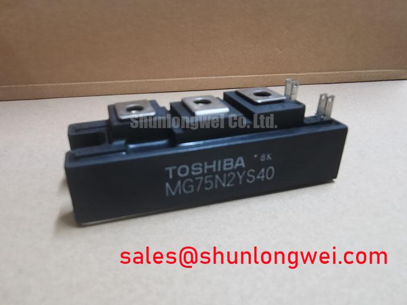
Assembly Integrity and Thermal Response of the MG75N2YS40
Measure the installed module’s case temperature during a controlled load change, then compare the trace with the heatsink temperature at the same location. A widening difference can point to a deteriorating thermal contact, restricted airflow, or a changed load profile; it does not, by itself, identify which one is responsible. For a replacement assessment, record the waveform and temperatures before removing the existing assembly so the commissioned installation has a useful baseline.
The 1200 V and 75 A ratings are Official Specifications, not permission to sustain any current at any case temperature. Junction temperature during a pulse depends on the starting temperature, losses, pulse duration, and the device’s transient thermal impedance. An engineering calculation using a multi-RC thermal model would require Toshiba thermal-impedance data and operating-point loss data for this exact part. Without those inputs, a numerical peak-junction estimate would be speculative. As a Design Consideration, compare measured switching and conduction conditions with the applicable device documentation before accepting an overload profile.
Inspect the module footprint, mounting surface, terminal positions, and available electrical clearance against the original assembly drawing. Keep the gate-drive loop compact to reduce parasitic coupling, but judge its final routing by measured gate and collector waveforms under the intended operating conditions. Ringing can reflect loop inductance, driver behavior, probe placement, or their interaction. ROHM’s IGBT technical overview provides useful background on IGBT technology; it is not a specification for the Toshiba module.
For parts comparison, MG300Q1US41 can be examined alongside MG75N2YS40, but a shared product category does not establish interchangeability. Check circuit configuration, electrical ratings, terminal layout, mounting geometry, and gate-drive requirements against the equipment documentation before deciding whether either part fits the assembly.
MG75N2YS40 Operational Boundaries: DC Bus Stress and Site Conditions
Capture the collector voltage at turn-off and compare its observed peak with the 1200 V Official Specification while the equipment operates across its expected DC-bus range. Include startup, shutdown, and fault-recovery events in the review where they can be tested safely. Minimize power-loop inductance to limit turn-off overshoot, then let the system designer establish the operating margin from measured switching behavior rather than an assumed percentage.
At a high-altitude installation, review the equipment’s cooling and insulation design separately from the semiconductor voltage rating. Atmospheric-neutron exposure and single-event burnout are specialized reliability questions; no altitude derating, FIT rate, or safe DC-bus threshold can be assigned to MG75N2YS40 from the specifications provided here. The appropriate Design Consideration is to obtain device-specific manufacturer reliability guidance if those effects are material to the site assessment. Do not treat the module’s rated blocking voltage as a published cosmic-ray reliability guarantee.
Trace the fault path on the actual power schematic before evaluating fuse coordination. A semiconductor fuse’s clearing behavior must be checked against prospective fault current and the protected circuit’s withstand limits; the module’s 75 A rating alone does not define an allowable fuse clearing energy or surge limit. If the power stage contains other devices, identify their functions before comparing protection requirements. For example, FS75R12KT3G is a separate module to assess within a relevant power-stage design, not an assumed rectifier stage or a direct substitute for this Toshiba part.
Keep gate-drive terminology tied to the device being tested. IGBT turn-on is assessed through its gate-emitter drive and switching waveform; thyristor trigger-current and trigger-voltage parameters do not describe this module’s commissioning test. Where a schematic also includes thyristors, evaluate their triggering independently. This prevents a fault investigation from applying one device family’s acceptance criteria to another.
Field Diagnostics During Battery and Inverter Power Swings
Trend case temperature, heatsink temperature, DC-link voltage, and switching waveforms through a repeatable charge-to-discharge transition. In a commercial string inverter or microgrid energy-storage assessment, changing power direction can alter device losses and thermal cycling, but the installation’s actual topology determines whether MG75N2YS40 occupies that power path. Confirm its position on the schematic before assigning a temperature excursion to battery cycling.
Compare a suspect phase or switching position with a known-good path under the same command and load conditions. Examine gate voltage at the device terminals with an appropriate measurement setup, then check collector-voltage behavior and current-sensor records. Gate oscillation may involve drive-loop routing, shared return impedance, or switching interaction; it should not be diagnosed from a single trace without checking probe grounding and the driver’s command signal. Adjustments to damping or drive strength are system-design decisions that require switching-loss and voltage-overshoot verification.
For preventive maintenance, log changes in heatsink fouling, airflow, terminal condition, and thermal-contact performance alongside the operating profile. This makes a rising temperature trend easier to investigate without attributing it automatically to the semiconductor. Maintenance note: De-energize and verify the DC link is discharged before touching module terminals or disturbing the gate-drive connection. The Field Engineer’s Handbook offers a broader reference for organizing test records and failure analysis; any service-life estimate still needs evidence specific to the installed equipment.
MG75N2YS40 Operational Boundaries: Thermal Interface and Mounting
Inspect the removed module’s contact pattern and the heatsink surface for dry patches, debris, uneven pressure, or displaced interface material. Clean and prepare the mating surfaces using the equipment’s approved procedure. A visible gap or an uneven transfer pattern calls for checking flatness, mounting hardware, and assembly sequence rather than applying more compound without investigation.
As a Design Consideration, use a continuous, thin thermal interface layer that accommodates the actual mating surfaces without creating excessive separation. A specific bond-line thickness cannot be assigned to MG75N2YS40 from the available Official Specifications. Likewise, use the mounting sequence and torque specified for the module and equipment hardware; tightening by feel risks uneven contact. After assembly, verify terminal security and compare the thermal response under a controlled load with the baseline recorded before removal.
If the equipment uses a temperature sensor near the module, identify what it measures before interpreting its reading as junction temperature. An NTC thermistor, for example, changes resistance with temperature, as described in this thermistor reference; that does not establish that MG75N2YS40 contains an NTC or that any nearby sensor reads junction temperature directly. During routine service, check for condensation and airflow changes as well as contact-temperature drift, then investigate a persistent trend against the equipment’s maintenance records.