

Content last revised on September 28, 2026
Benchtop Waveform Tuning: Mitigating Stress via Dynamic Gate Impedance Control for Robust Operation
Begin bench evaluation with the power stage isolated from the full-energy DC source. Confirm the gate-driver output at the module terminals rather than measuring only at the driver board. The probe reference, return conductor, and test-loop geometry can materially alter the observed waveform. When a high-voltage IGBT module is switched at high current, common-source inductance, gate-loop inductance, driver output impedance, and collector-to-gate coupling interact. The resulting waveform may include gate ringing, delayed turn-off, or an unintended rise in the opposite device’s gate voltage.
Design Consideration: A dedicated active Miller clamp can help hold the inactive gate at its intended off-state potential during a rapid collector-voltage transition, provided the clamp path is physically close to the driver return and the driver’s common-mode behavior has been verified. Some high-power converter designs also evaluate a negative gate bias, often within the driver manufacturer’s permitted range, to improve off-state immunity. The appropriate value is system-determined and must be checked against the CM1500HC-66R gate-emitter limits, driver isolation rating, startup sequence, and fault behavior. The supplied product parameters do not establish a universal negative-bias setting.
Dynamic gate impedance control is best treated as a waveform-tuning method rather than a fixed prescription. A low impedance during the initial turn-on interval can reduce delay and switching loss, while a controlled impedance during the high-voltage transition can moderate ringing and electromagnetic interference. The final setting depends on gate charge, bus voltage, load current, commutation path, driver capability, and stray inductance in the installed converter. Designers should compare the gate-emitter waveform at the module pins with the collector-emitter waveform and the complementary device’s gate waveform during double-pulse testing.
High dv/dt induced cross-conduction is not confirmed by one abnormal waveform alone. Review the complementary gate signal, dead-time implementation, driver supply stability, isolation-channel propagation, and the physical distance between power and control returns. If the opposite gate rises during the active device’s transition, verify whether the rise is caused by Miller coupling, common return movement, probe error, driver saturation, or an incorrect clamp connection. The test should be repeated with a known-good measurement arrangement before changing the gate network.
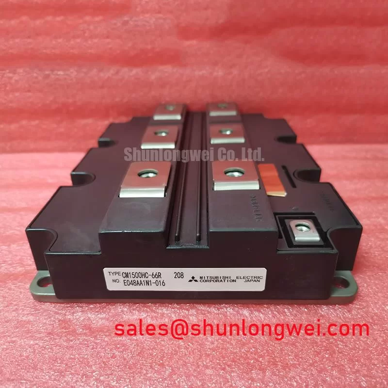
When evaluating a replacement in an existing PCS, compare the original module’s gate-driver topology with the CM1500HC-66R interface and terminal arrangement. The CM50DY-28H may appear in related sourcing evaluations, but electrical ratings, pin configuration, switching behavior, thermal requirements, and mechanical fit must be confirmed independently before considering any alternative. A catalogue resemblance is not a replacement qualification.
During bench tuning, record the DC-link voltage, phase current, gate-emitter voltage, collector-emitter voltage, switching temperature, and fault response in the same test record. Oscilloscope traces should be taken at a safe, repeatable operating point and then repeated across the converter’s intended operating range. This provides a more useful basis for design decisions than selecting a gate resistor from a nominal value alone.
CM1500HC-66R Operational Boundaries: Evaluating DC-Bus Low-Inductance Laminated Busbar Design Limits
The DC-link connection deserves the same scrutiny as the gate circuit. At turn-off, the voltage overshoot is influenced by the DC-bus voltage, commutation current, switching rate, and total stray inductance in the high-current loop. In engineering terms, the overshoot contribution follows the relationship between inductance and current change, so a busbar that looks mechanically short may still produce excessive stress if its forward and return paths are separated or poorly coupled.
Design Consideration: Use a compact, symmetrical laminated busbar arrangement to reduce the area of the commutation loop, then verify the resulting peak collector-emitter voltage with a properly rated differential probe during switching tests. The target parasitic inductance is determined by the converter topology, switching conditions, device limits, and clamping strategy; it should not be assigned from a generic number without a validated layout and measurement method. The measured peak must remain within the applicable module and system voltage boundaries under the worst credible combination of bus voltage, current, temperature, and commutation conditions.
Film capacitors placed close to the switching loop can provide a lower-inductance local current path than a remote bulk capacitor. Their selection is a system design task involving ripple current, self-resonant behavior, insulation coordination, physical clearance, temperature, and the expected switching spectrum. A larger capacitance value does not automatically provide better transient control if the mounting path introduces excessive inductance. The capacitor terminals, module terminals, and laminated conductors should be examined as one physical loop.
Freewheeling diode reverse recovery can increase the current excursion seen by the switching device and can add both voltage stress and radiated noise. The effect depends on diode technology, junction temperature, commutation current, gate timing, and circuit inductance. If a waveform shows a sharp recovery event, measure the current path and verify whether the event is associated with diode recovery, probe bandwidth, busbar coupling, or an interaction between parallel commutation paths.
Snubber evaluation should follow the measured energy and ringing frequency rather than rely on an assumed capacitor value. A practical engineering recommendation is to identify the dominant ringing mode with a controlled switching test, then assess whether an RC, RCD, or other clamp network reduces the peak without creating unacceptable dissipation or EMI elsewhere. The final snubber component values should be selected from measured conditions and verified for pulse power, temperature rise, insulation, and fault operation.
For a centralized battery storage PCS, the DC bus is also affected by the battery rack interface, pre-charge circuit, contactor timing, isolation monitoring, and converter control response. Engineers evaluating this module in a LiFePO4-based system can review the general battery chemistry context through Lithium Iron Phosphate battery storage chemistries. The battery management system remains a separate system-level control and protection domain; its architecture can be reviewed through Battery Management System architecture. Neither reference changes the official electrical ratings of the CM1500HC-66R.
CM1500HC-66R Thermal-Electrical Optimization: Fault-Clearing Dynamics and Desaturation Tuning
Desaturation protection should be evaluated as a coordinated protection chain involving the gate driver, sensing path, blanking behavior, soft turn-off function, fault latch, and system controller. The CM1500HC-66R rating identifies the device class and its official voltage and current values, but it does not establish a universal desaturation delay, short-circuit withstand interval, or fault-clearing sequence. Those values require the applicable manufacturer documentation and validation on the actual converter hardware.
A two-stage soft turn-off approach can be considered where an abrupt gate discharge would otherwise create excessive inductive voltage. The first stage limits the rate of current reduction, while the later stage brings the gate to the defined off-state. The driver designer must verify that this approach clears the fault quickly enough for the device and system protection requirements while avoiding a second voltage excursion caused by the commutation inductance. The selection is conditional on the gate-driver design, fault current, bus voltage, temperature, and layout.
When a desaturation event occurs during testing, capture the desaturation input, gate-emitter voltage, collector-emitter voltage, phase current, driver supply, and fault-output timing on the same time base. Inspect the sensing diode or current-sense interface, blanking network, isolation channel, and fault latch behavior. An unexpected trip may involve noise coupling, insufficient measurement margin, a driver supply disturbance, or a real overcurrent condition. A missed trip requires equally careful review because the absence of a fault signal does not prove that the switching device is operating safely.
Thermal and electrical behavior must be reviewed together. Conduction loss raises junction temperature, while switching loss changes with current, voltage, gate resistance, commutation conditions, and temperature. The heatsink or cold plate, interface material, mounting pressure, airflow or coolant path, and temperature-sensor location should be inspected during the same test campaign. The official 1500.0 A current rating should not be interpreted as a guaranteed continuous current under every cooling arrangement or waveform.
Designers should verify the fault response at controlled current levels before applying full system energy. Test cases may include an inhibited gate command, an intentionally interrupted cooling condition, an abnormal driver supply, and a controlled overcurrent event, subject to the laboratory’s safety procedures. The goal is to confirm that the driver detects the condition, limits the switching transition, communicates the fault, and prevents an automatic restart that the battery PCS control system has not authorized.
For additional measurement discipline covering power-module testing, fault analysis, and reliability-oriented inspection, consult the Field Engineer’s Handbook. It should supplement, not replace, the component manufacturer’s datasheet, the converter safety design, and the site commissioning procedure.
Assembly Integrity and Layout Architecture: Implementing PCB Gate-Loop Symmetry
Route the gate-drive loop as a compact send-and-return circuit and keep it physically separated from the high-current collector and emitter paths. The auxiliary emitter or control return should not share a long, high-current copper route with the power emitter connection. Shared impedance can move the apparent gate reference during switching and may produce oscillation, false driver feedback, or inconsistent turn-on and turn-off behavior between parallel paths.
Where the module provides separate control and power terminals, follow the manufacturer’s terminal definition and the original converter’s verified connection method. Do not infer a Kelvin-style return, pin assignment, or internal topology from the package outline alone. The PCB interface, busbar, driver board, and module terminals should be checked as a complete assembly, especially when adapting an existing power stack to the CM1500HC-66R.
Gate-loop symmetry matters when multiple switching positions operate in parallel or when the upper and lower devices in a leg have different physical distances to the driver. Match the outgoing and return paths as closely as the mechanical design allows, avoid unnecessary vias and narrow necks, and keep the driver return away from pulsed power copper. These are design considerations rather than CM1500HC-66R factory specifications. The final layout must be validated by probing every relevant gate and emitter reference under the intended switching conditions.
Mechanical assembly can also affect electrical repeatability. Confirm that the module base, thermal interface, heatsink or cold plate, busbar supports, and terminal fasteners remain aligned without imposing side load on the power terminals. Apply the equipment manufacturer’s specified fastening procedure and inspect for uneven contact, damaged threads, displaced interface material, and conductor movement after thermal cycling. ⚠️ Field Alert: isolate and discharge the DC link before removing cables or probing the module, and verify the absence of hazardous voltage with an approved measurement procedure.
After assembly, perform a cold-state inspection, insulation and continuity checks appropriate to the converter, gate-driver power-up verification, and a staged switching test before reconnecting the battery system. Review the waveform at the module terminals after any change to busbar position, driver-board mounting, gate resistance, snubber placement, or cooling hardware. This final comparison is essential because a mechanically acceptable installation can still change the parasitic electrical network enough to alter switching stress.