

Content last revised on September 23, 2026
PWB60A40 Operational Boundaries: Evaluating Reverse Recovery Charge Temperature Coefficient Limits
During a soft-starter inspection, first record the line voltage, motor nameplate current, firing arrangement, bypass contactor sequence, and the protective fuse part number. The PWB60A40 carries an official voltage rating of 2500.0 V and an official current rating of 60.0 A, but those figures alone do not establish the allowable reverse-recovery stress in a particular commutation circuit. The system engineer should verify the relevant diode or thyristor recovery characteristics from the correct NIEC technical document before treating the module as interchangeable.
Reverse recovery is best evaluated at the actual operating temperature and current waveform expected in the equipment. Use an appropriately rated differential voltage probe and current probe, with the measurement loop arranged to avoid adding excessive stray inductance. Observe the current transition when the conducting device is commutated and compare the recorded peak, duration, ringing, and recovery behavior with the approved design envelope. Temperature should be recorded at the module mounting surface and, where available, at the approved case reference point. A change in recovery behavior with temperature may affect switching loss and conducted or radiated disturbance, but no temperature coefficient or recovery limit should be assigned to this model without a sourced data sheet.
Fuse coordination requires the same discipline. The PWB60A40 page data supplied for this product does not include an I²t table or a specific fuse pairing. The maintenance engineer should therefore compare the original fuse class, pre-arcing characteristic, prospective fault current, clearing time, and manufacturer coordination information. A fuse with a suitable current label may still be unsuitable if its clearing behavior does not protect the semiconductor during a prospective short circuit. The final selection remains a system protection decision.
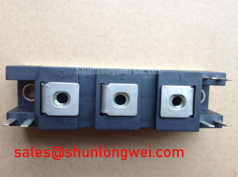
Terminal work should be completed with the equipment fully isolated and discharged. Clean contact surfaces, inspect for discoloration, and verify that the conductor arrangement matches the original circuit. Do not infer terminal polarity, internal topology, or permissible tightening torque from the package description alone. The SanRex power semiconductor module reference provides useful industry context for module handling and power-semiconductor applications, while the power module architecture reference explains why package isolation and internal topology must be checked against the actual circuit.
When a cross-reference is being considered, compare voltage class, continuous current conditions, commutation duty, isolation construction, terminal geometry, and gate-drive requirements as separate items. The PGH50N16 may be reviewed as a neutral cross-model reference, but its electrical ratings and internal configuration must be assessed independently rather than treated as a direct replacement for the PWB60A40.
Assembly Integrity and Layout Architecture: Preventing Localized Gate Hotspot Burnout for PWB60A40
Before applying a firing pulse, trace the complete gate-control path from the isolating driver to the module terminals. Confirm the intended gate and cathode references from the original documentation. The supplied product data identifies the PWB60A40 as an isolated power module, but it does not confirm a Kelvin emitter, auxiliary cathode, dedicated sense terminal, recommended negative gate bias, gate resistance, pulse amplitude, or pulse-width range. These details must not be assumed from the package category.
Gate-drive evaluation should use an isolated measurement method that captures the voltage directly at the module terminals during the complete firing sequence. Inspect the leading edge, pulse stability, return path, and behavior during commutation. A rapid gate-current transition can interact with common-mode inductance, driver output impedance, and stray coupling. If the control design uses a firing condition described by the project specification as diG/dt greater than 1 A/µs, the engineer should verify that condition against the approved NIEC gate-drive data rather than treating it as a universal PWB60A40 requirement.
Back-porch holding current and multi-pulse firing schemes also require confirmation from the application documentation. A holding pulse that is adequate at one temperature or line condition may not provide the same margin during motor acceleration, supply disturbance, or driver isolation changes. Check the gate waveform while the power path is carrying the expected load, not only with the motor disconnected. Any observed gate ringing, pulse interruption, or unexpected common-mode displacement should be compared with a known-good channel and investigated through the driver, isolation barrier, return conductor, and module connection.
Keep the gate loop physically separate from high-current commutation conductors wherever the cabinet layout permits. This is a Design Consideration intended to reduce coupled noise; it is not a published PWB60A40 construction requirement. If the assembly includes an auxiliary emitter or Kelvin-style connection, use it only when the manufacturer terminal diagram confirms its function. A standard emitter or cathode terminal must not be relabeled as a Kelvin reference by assumption.
⚠️ Maintenance Note: Check the module contact temperature trend and cooling-air path during scheduled service, because a clean heatsink and secure terminal connection are basic prerequisites for meaningful gate-drive troubleshooting.
The related FRS200CA100 can be reviewed as a separate front-end or complementary topology reference when examining the complete soft-starter power path. Its specifications must be verified independently, and its presence in the same system does not establish electrical compatibility with the PWB60A40.
Assembly Integrity and Layout Architecture: Implementing Turn-On Current Rise Limiting for PWB60A40
Inspect the turn-on waveform at the module terminals and at the motor-side output before changing any snubber or series impedance. The objective is to distinguish a control-timing issue from a power-loop layout issue, supply imbalance, motor inrush behavior, or an incorrectly selected protection component. Use synchronized voltage and current measurements across all three phases where possible. Compare phase symmetry, firing angle progression, current rise, ringing, and the point at which the bypass path becomes active.
RC snubbers and series saturable reactors are system-level components. The supplied PWB60A40 information does not specify an Rs value, Cs value, reactor characteristic, dv/dt limit, or recommended network. The system designer should select and validate these parts from measured switching behavior, the complete circuit impedance, capacitor voltage rating, resistor pulse capability, and the applicable NIEC application guidance. The design principle is to limit unwanted voltage transients and current rise while preserving the intended firing sequence; the final component values must be established by test.
When inspecting an existing snubber, look for capacitor swelling, resistor discoloration, cracked insulation, loose fasteners, and evidence of repeated pulse overheating. Measure the components only after isolation and discharge, using instruments suitable for the component voltage class. A reading outside the expected maintenance tolerance may indicate damage, but it does not identify the original failure mechanism by itself. Review the oscilloscope record, fuse condition, motor acceleration time, line balance, and bypass-contact timing together.
Parasitic loop inductance should be minimized where it contributes to turn-on overshoot or commutation ringing. This is a Design Consideration, not a PWB60A40 dimensional specification. The physical arrangement should be reviewed by the system engineer, who must verify voltage peaks, current rise, insulation clearances, and thermal behavior during switching tests. Do not add a gate resistor, negative cutoff bias, snubber, or reactor solely from a generic application diagram without confirming the module’s approved gate and protection requirements.
For maintenance teams, terminal inspection should include conductor crimp condition, lug alignment, signs of localized heating, and the integrity of insulating barriers. Any replacement hardware should preserve the original creepage and clearance arrangement. The isolated package classification supports an isolation-based assembly concept, but it does not provide a complete insulation coordination approval for the finished soft starter.
Assembly Integrity and Layout Architecture: Implementing Non-Repetitive Surge On-State Current for PWB60A40
Surge evaluation begins with the motor-start record and the protection record. Capture the number of starts, acceleration duration, line voltage, phase current, ambient conditions, heatsink condition, and fuse operation. The PWB60A40 is specified here at 60.0 A and 2500.0 V, yet no non-repetitive surge current rating, ten-millisecond half-cycle value, junction-temperature limit, or transient thermal impedance curve has been provided. Those missing values are essential before a 10 ms half-cycle surge claim can be made.
Do not substitute the continuous current rating for a surge rating. A short-duration current event can be limited by junction heating, bond and terminal stress, fuse clearing behavior, motor impedance, and the time required before reverse voltage is reapplied. The engineer should obtain the official ITSM and associated repetitive surge conditions for the exact PWB60A40 revision, then compare them with the measured waveform and protection coordination of the soft starter.
Transient thermal impedance should be treated as a waveform-dependent property rather than a fixed temperature allowance. If the manufacturer provides a Zth curve, use the actual pulse duration and duty pattern to estimate junction response, then validate the result with case-temperature measurements and controlled switching tests. If no curve is available, avoid calculating a numerical junction margin from assumed values. The result should be reviewed against the approved maximum junction temperature and the complete cooling path, including interface material condition, heatsink flatness, airflow, and enclosure temperature.
Before reverse voltage is reapplied, verify the commutation interval, line phase relationship, firing control sequence, and measured residual current. A failed or delayed bypass contactor can change the semiconductor duty substantially. Inspect the module for package cracking, terminal discoloration, mounting movement, and thermal interface degradation, but do not assign a single cause from visual evidence alone.
Reliability planning may also benefit from the technical context in Wide Bandgap Revolution, particularly when comparing broader semiconductor switching and thermal design principles. That reference does not alter the published PWB60A40 ratings or certify the module for a particular soft-starter topology.
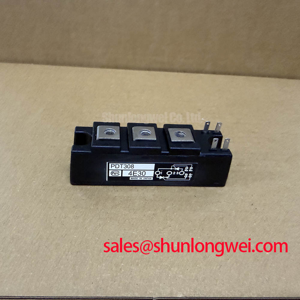
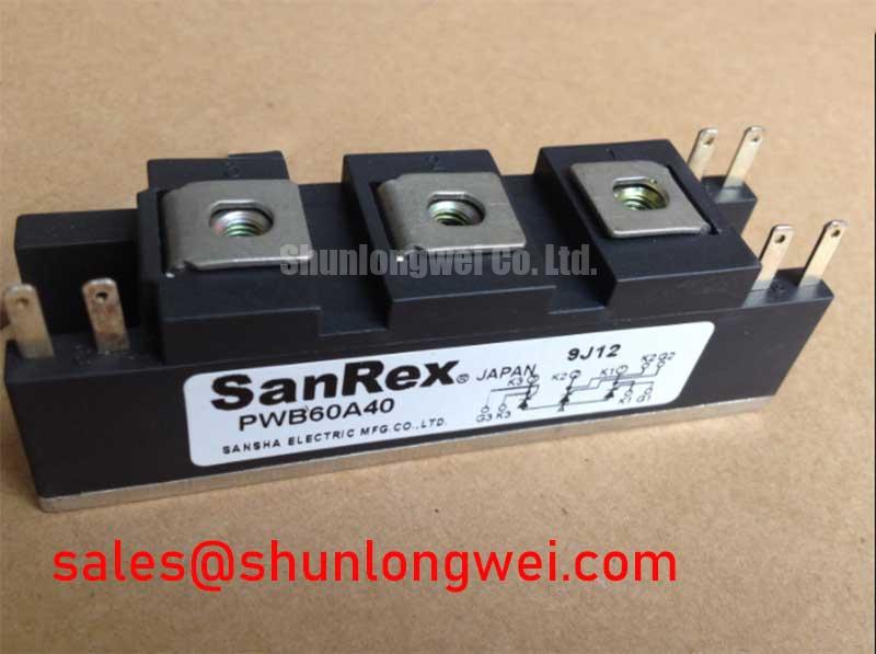
For procurement and field replacement, record the complete model marking, manufacturer reference, voltage class, current class, package type, terminal arrangement, and the host equipment application. The PWB60A40 should be released for service only after the original circuit documentation confirms the required electrical, thermal, mechanical, and protection conditions.