

Content last revised on November 6, 2026
QM50DY-H Thermal-Electrical Optimization: Base-Drive Resistance Calibration for Practical Tuning
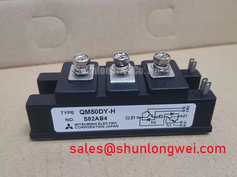
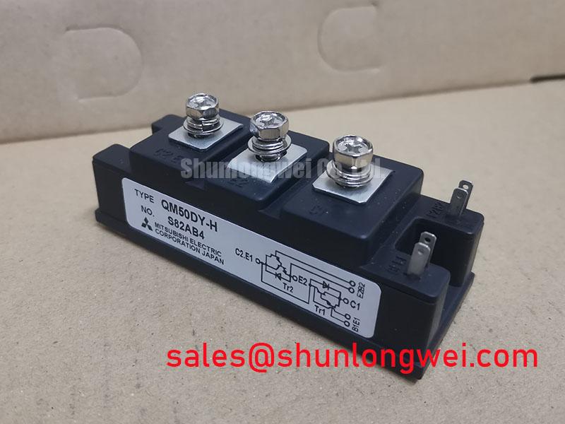
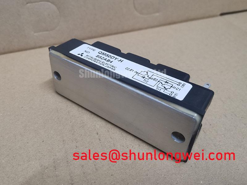
Manufacturer: Mitsubishi Electric | Part Number: QM50DY-H | Class: Power Transistor / Darlington Module | VCES: 600.0 V | IC: 50.0 A | Package: Isolated Darlington Module | Configuration: Darlington Power Module
When a legacy inverter board shows excessive turn-off ringing after a QM50DY-H replacement, I first separate the base-drive loop from the power loop and inspect the base-emitter waveform at the module terminals. The objective is to adjust the external base-drive network without confusing a layout problem with a resistor problem. The QM50DY-H carries an official Collector-Emitter Voltage (VCES) rating of 600.0 V and an official Continuous Collector Current (IC) rating of 50.0 A; these ratings define the component identification baseline, not an automatic operating limit for every switching condition.
Use separate turn-on and turn-off base-drive paths only when the board architecture allows independent control. Adequate turn-on base current can reduce conduction overlap, while a controlled turn-off profile can help manage collector voltage overshoot and ringing. The correct balance is system-dependent: monitor base-emitter voltage, collector-emitter voltage, collector current, and device temperature under the actual DC-link and motor-load conditions. If the measured waveform changes substantially when the oscilloscope ground connection is moved, investigate measurement-loop inductance and common-mode ground bounce before changing the resistor network.
As a design consideration, keep the base-drive return physically close to its corresponding emitter return. Where the module provides a dedicated emitter connection for the driver reference, route it separately from the high-current commutation path; where no separate terminal is available, the control board must account for shared emitter inductance. Base-drive isolation, turn-off base-current handling, and common-mode shielding should be selected by the system designer after checking the original drive topology. Do not assume that a drive arrangement used in another inverter platform is suitable.
For a field retrofit, record the original resistor network, base-driver supply arrangement, and fault behavior before fitting the replacement. Then compare the new switching waveform with the known-good board at reduced test energy. Persistent overshoot that remains after reasonable base-drive adjustments usually points toward DC-link stray inductance, busbar geometry, diode recovery, or probe placement rather than the resistor value alone. Maintain practical creepage and clearance around the power terminals, base wiring, and control isolation barrier according to the applicable equipment standard.
Field Alert: De-energize the DC link and verify discharge before inserting, removing, or probing the module, because hazardous stored energy may remain after the motor stops.
Benchtop Waveform Tuning: Mitigating Stress via Regenerative DC-Bus Voltage Surge Dissipation on QM50DY-H
Regenerative braking testing begins with the motor and load profile, not with the braking transistor label. During deceleration, kinetic energy returns through the inverter and raises the DC-link voltage; the braking transistor and ballast resistor must absorb the resulting energy without exceeding their electrical, thermal, or pulse-duty boundaries. Treat the QM50DY-H as a Darlington transistor module; do not assume a dual-half-bridge arrangement. Confirm the actual terminal arrangement and switching path against the equipment schematic and applicable module documentation before assigning the part to a braking branch.
Dimensioning the braking network requires the deceleration energy, repetition rate, resistor pulse capability, allowable DC-link excursion, switching duty, cooling path, and protection response to be considered together. A resistor that survives one test pulse may still accumulate heat during repeated spindle stops. For a compact industrial inverter or high-speed CNC spindle drive, capture the DC-link waveform during the fastest expected stop and correlate it with the braking command. The oscilloscope record should show whether the surge is caused by insufficient energy absorption, delayed braking command, wiring inductance, or an unexpectedly regenerative load.
When parallel modules or parallel transistor paths are considered, symmetrical busbar geometry and matched base-drive paths are design considerations. Current sharing depends on device characteristics, operating conditions, circuit layout, base-drive timing, emitter coupling, and thermal placement. Do not assume that identical part markings produce identical transient current distribution. Verify each branch during controlled switching tests and inspect the hottest electrical and mechanical locations, not only the average heatsink temperature.
The same thermal reasoning applies to a bidirectional DC-DC battery interface when its switching devices are selected for that topology. Repeated power reversal creates thermal cycling in the semiconductor, baseplate, interface material, busbar, and resistor assembly. Designers should correlate junction-temperature estimates with the transient thermal impedance network, pulse duration, switching frequency, and cooling response. The supplied product data confirms the 600.0 V collector-emitter voltage and 50.0 A continuous collector current, but it does not establish a universal braking-energy rating or lifetime figure for a complete drive.
For physical integration, minimize the high-current commutation loop area and keep the braking resistor connection away from sensitive base-drive and current-sense wiring. A busbar layout with equal electrical path length is preferable when branches are paralleled. Powerex provides an industry reference point for high-power semiconductor module practices through its Powerex High Power Semiconductor Modules resource; the final equipment design must still be validated against its own protection, thermal, and EMC requirements.
Benchtop Waveform Tuning: Mitigating Stress via Damping Commutation Oscillations During Turn-On on QM50DY-H
Commutation oscillation during turn-on is best investigated by viewing the freewheeling diode current, where a diode is present, and the transistor collector-emitter voltage at the same time. The diode’s peak reverse-recovery current, Irrm, and the steepness of its reverse-recovery transition can interact with bus inductance and the turn-on base-drive path. The resulting ringing may increase voltage stress, acoustic noise, and radiated or conducted emissions, but its exact source must be established from the measured commutation waveform.
Start with a short, properly compensated differential-voltage connection and a current measurement method suitable for the expected pulse. Compare the waveform with the base-drive command, then vary the turn-on base resistance as a controlled bench parameter. A higher base resistance can moderate the current transition and reduce excitation of parasitic resonance, while an unnecessarily slow transition increases switching loss. An RC snubber can be evaluated when the ringing frequency and damping requirement are understood; its placement should be close to the switching nodes it is intended to control, with the component loop kept compact.
Do not place a snubber across an undefined pair of terminals. On an isolated module, identify the collector, emitter, diode, and base terminals from the applicable connection drawing and the original board circuit. If the base-drive return shares a noisy power return, common-mode ground bounce can appear as a false base-drive disturbance. Separate the control reference from the high-current return where the package and board design permit it, and use shielded or tightly coupled base-drive routing only as part of a complete isolation and EMC strategy.
When a separate emitter sense connection is available, route it independently to the driver reference and avoid carrying load current through that trace. If the QM50DY-H installation does not provide such a terminal, the system engineer should account for the shared inductive voltage in the base-drive design. The appropriate snubber value, base resistance, and damping location are determined by measured ringing, switching loss, thermal response, and the required DC-link voltage margin during the actual operating sequence.
For replacement evaluation, the neutral comparison page for PM50CSD060 can be reviewed when the equipment designer is assessing another module family, but electrical, mechanical, terminal, and drive compatibility must be checked independently. Thermal implementation should also consider the complete path from semiconductor junction through the interface and heatsink to ambient; the From Chip to Air Technical Reference provides a relevant engineering framework for that assessment.