


Content last revised on September 23, 2026
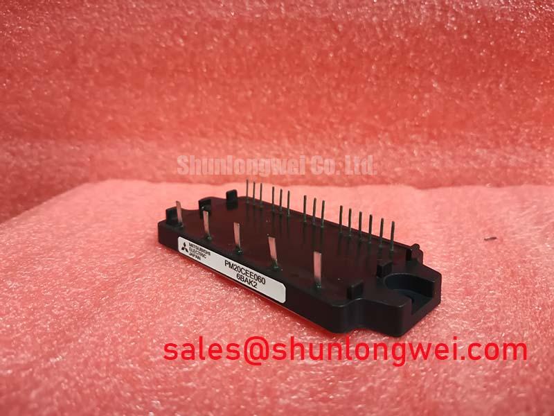
Preventing Spurious Faults: Fault-Clearing Dynamics: Type-I/II Desatur Guidelines for PM20CEE060
A drive that repeatedly trips during acceleration, deceleration, or abrupt axis reversal should be assessed at the protection interface before the PM20CEE060 is treated as the sole cause. Start with an isolated visual inspection of the driver board and module control connection. Check for damaged connector retention, contamination near low-voltage control traces, cracked solder joints, weakened gate-drive supply connections, and signs that a prior fault has stressed nearby resistor networks or optocoupler circuits.
Desaturation protection is commonly used in IGBT drive systems to identify a short-circuit-like condition by monitoring the switching device voltage while it is commanded on. Type-I and Type-II desaturation approaches differ in how the event is sensed and managed within the protection architecture. The exact fault threshold, blanking interval, response sequence, and driver behavior are system-defined characteristics, not published operating guarantees for this PM20CEE060 listing. Engineers should verify these values from the original servo-drive schematic and the installed gate-driver documentation.
When a desaturation event occurs, the shutdown path requires particular attention because a fast interruption of current through an inductive load can create a voltage excursion. A controlled soft turn-off sequence is often evaluated as a Design Consideration where the application must reduce stress during a detected fault. The aim is to move the affected switching device from conduction to blocking in a managed manner while the surrounding clamp, DC-link, load path, and protection network absorb the transient according to the system design.
In practical troubleshooting, capture the fault sequence with appropriately rated differential voltage and current measurement equipment. Observe the command input, gate command, fault output, DC-link behavior, and phase-current response together. A fault flag that appears before the intended gate transition may indicate control noise, supply instability, an incorrect blanking relationship, or an issue elsewhere in the drive. A fault flag that appears only during high-torque operation may instead justify checking the motor cable, load condition, busbar joints, cooling performance, and the integrity of the current-sensing path.
PCB clearances, creepage distances, and routing separation should be reviewed against the equipment’s applicable insulation and safety requirements. Design Consideration: keep sensitive protection-sense paths physically separated from high-current commutation loops where possible, because induced noise can interfere with a desaturation measurement. The system engineer should verify this with switching tests under realistic bus voltage, load current, ambient temperature, and motor-cable conditions.
⚠️ Maintenance Note: During scheduled service, monitor terminal and heatsink contact temperature rise under comparable operating load, then confirm that cabinet airflow paths remain free of dust buildup and blocked filters.
Preventing Spurious Faults: Turn-Off di/dt Induced V_peak Clamping and Guidelines for PM20CEE060
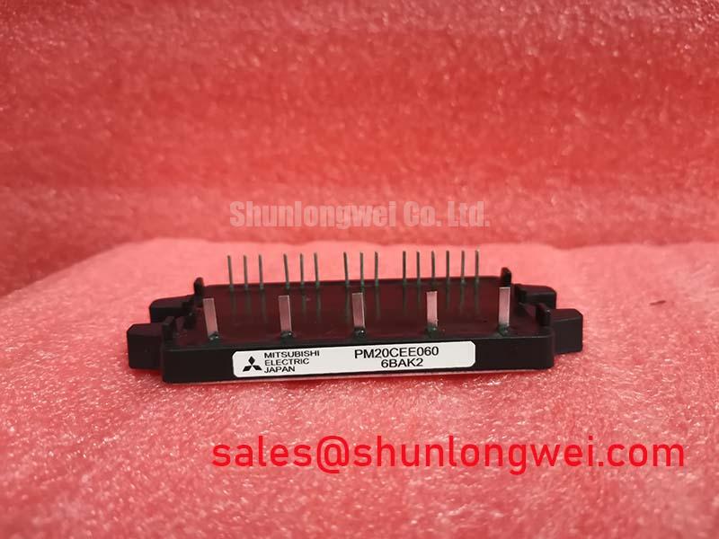
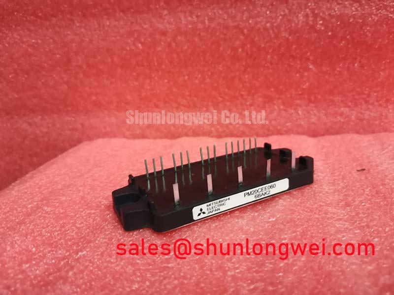
The official 600.0 V rating is an essential identification boundary for PM20CEE060, but the actual switching waveform in an installed converter depends on the complete power loop. During turn-off, the peak voltage is governed by the DC-link voltage plus the voltage generated across stray inductance as current changes. In engineering terms, the relationship follows Vpeak as VDC plus loop inductance multiplied by current slew rate. This is an Engineering Calculation principle, not a module-specific clamp specification.
For a servo amplifier or compact motion-control inverter, the highest-risk loop usually includes the DC-link capacitor connection, power terminals, module current path, and return conductor. Design Consideration: minimize the loop area and preserve a short, symmetric power path to suppress inductive overshoot during commutation. The acceptable inductance, capacitor selection, clamping approach, and switching slope must be established by the actual system design and confirmed by waveform measurement rather than assumed from module current rating alone.
If a repair follows damage around the DC-link capacitors, inspect capacitor mounting hardware, copper straps, busbar surfaces, soldered joints, and any added suppression components. A loose connection can alter the commutation path and produce unstable switching behavior. Likewise, a capacitor with degraded electrical condition can affect local energy support and increase transient sensitivity. These observations do not establish a single failure cause; they identify areas that warrant measured comparison against a known-good drive stage.
Switching frequency can also influence the thermal operating condition because switching losses, conduction losses, heatsink capability, enclosure airflow, and duty cycle interact. A drive that operates acceptably at one command profile can run significantly warmer under repetitive motion cycles, rapid reversals, or sustained high-torque load. Engineering Recommendation: validate module and heatsink thermal behavior during the actual production duty cycle, including the cabinet temperature and cooling-fan condition, instead of using a general frequency-based assumption.
For preventive maintenance, remove dust from heatsink fins, blower inlets, protective grilles, and cabinet air channels using a method appropriate to the facility’s electrical safety procedure. Examine thermal interface material during service when the module is removed. Uneven residue, hardening, void-like contact patterns, or contamination may justify a controlled replacement using the original equipment assembly method. The PM20CEE060 listing does not provide an official mounting torque, thermal grease thickness, or heatsink specification, so those values should be taken from the equipment manufacturer’s service documentation.
In systems where the converter front end uses separate rectification hardware, the relationship between the DC supply stage and inverter stage should be reviewed rather than treating them as isolated repairs. A module such as CM100DY-12E may be evaluated as an associated power-stage item in relevant equipment architectures, subject to the original circuit topology, electrical ratings, mounting arrangement, and service documentation.
Benchtop Waveform Tuning: Mitigating Stress via High dv/dt Cross-Conduction Shoot-Through on PM20CEE060
Before energizing a repaired drive at full operating conditions, begin with a controlled bench inspection of the driver board, command isolation interface, auxiliary supplies, and gate-return routing. Verify that the original PM20CEE060 control connection is fully seated and that no conductors have been trapped beneath covers or pressed against high-voltage terminals. If the equipment provides documented diagnostic outputs, use them to confirm the intended fault state before applying the normal DC-link operating condition.
High dv/dt switching can couple energy into nearby gate-control paths. In a bridge arrangement, this coupling can contribute to unintended turn-on of a device that should remain off, potentially creating cross-conduction. The susceptibility depends on the installed driver topology, the gate-emitter return impedance, power-loop geometry, parasitic capacitances, cable routing, and the condition of the driver supply. It cannot be determined from the PM20CEE060 voltage and current ratings alone.
Design Consideration: a low-impedance off-state gate path, an active Miller clamp where supported by the driver architecture, and an appropriately controlled negative off-state gate bias are commonly assessed to improve immunity against dv/dt-induced turn-on. The required bias magnitude, gate resistance, clamp timing, and dead-time behavior must be selected from the original system requirements and verified through measured switching tests. Applying a generic gate-drive setting without reviewing the original driver limits can create new reliability or protection problems.
Oscilloscope work should focus on correlation rather than one isolated waveform. Compare the intended PWM command, driver output, gate command, phase voltage, DC-link voltage, and current response. Ringing at the gate signal can arise from several sources, including probe setup, return-path coupling, board layout, connector condition, damaged damping components, or the driver circuit itself. Use a measurement method appropriate for high-voltage switching environments and compare results with a known-good signal path whenever possible.
For high-dynamics multi-axis CNC and robotics servo equipment, the PM20CEE060 may be considered during compatibility evaluation where the original drive was designed around the same electrical class and physical interface. Engineers should verify motor-current demand, overload profile, axis regeneration behavior, controller fault logic, enclosure cooling, and the complete module connection arrangement before commissioning. The fact that two modules share a voltage class does not establish direct interchangeability.
When reviewing alternative repair paths, CM300DXDX1-24A is a separate power-module reference that can be reviewed against system requirements. Its presence in a parts evaluation does not imply a direct substitution for PM20CEE060. Electrical topology, control interface, physical fit, thermal path, protection coordination, and original equipment requirements must all be checked independently.
PM20CEE060 Circuit Protection & Reliability: Calibrating Auxiliary Emitter Return Trace Separation
Gate-driver stability depends heavily on how the low-level control return relates to the high-current power return. In installations that provide a dedicated auxiliary emitter or control-return reference, the original driver-board routing should be preserved. A shared section of high-current emitter return can develop voltage disturbance during switching, and that disturbance can appear in the gate-control reference. The resulting waveform may contribute to gate oscillation, reduced noise margin, irregular protection behavior, or unexpected switching timing.
Engineering Recommendation: keep the driver reference path distinct from the main high-current return path wherever the original module and driver topology support that arrangement. The purpose is to reduce mutual coupling from load-current commutation into the gate-control loop. Exact trace geometry, connection points, return-path length, and routing constraints are determined by the existing equipment design. They should be verified against the board artwork and measured during switching tests rather than recreated from generic layout rules.
When a field repair includes replacement of damaged copper links, connector tails, or driver-board conductors, inspect whether the repair has altered the original return hierarchy. A seemingly small reroute can change the path followed by transient current. Check continuity, connection security, spacing from power conductors, and whether a service action has accidentally tied a sensitive control return into a noisy high-current path. If the drive operates inconsistently after repair, investigate the gate-reference waveform and fault signal integrity before changing protection settings.
Long-term operation also depends on disciplined environmental maintenance. Condensation risk, contaminated cabinet airflow, loose terminals, and aging thermal interface material can each affect equipment behavior without producing the same diagnostic pattern. Keep the enclosure dry within its specified operating environment, inspect cooling hardware during planned downtime, and verify mechanical connections according to the original equipment service procedure.
Where a repair team is studying off-state gate-control behavior in a broader IGBT system, Evolution of Negative Off-Bias Gate Drive Circuits provides relevant technical background. Any negative-bias implementation must remain within the installed gate-driver and equipment requirements, with final validation performed on the complete system under controlled conditions.