


Content last revised on September 14, 2026
Benchtop Waveform Tuning for SEMIX403GB128DS Using Symmetrical Busbar Geometry
When this module is evaluated in a commercial string inverter or microgrid energy storage converter, begin with the complete commutation path rather than the module alone. Record the DC link voltage, gate command, collector emitter voltage, collector current, and freewheel diode current during controlled switching tests. A high voltage probe and current probe should be connected with the shortest practical measurement loop so that probe inductance does not become part of the apparent overshoot.
Turn off voltage stress is influenced by the DC link voltage and the inductive voltage generated by the switching loop. In engineering terms, the peak voltage rises with stray inductance and current change rate, so a symmetrical planar busbar arrangement is a design consideration for reducing unequal current paths and limiting ringing. The target inductance, clearance, snubber value, and switching speed are system determined. Engineers should establish them from measured waveforms, the module documentation, insulation requirements, and the voltage margin required by the converter.
Place the high frequency DC link decoupling close to the power terminals and keep the outgoing and returning conductors physically adjacent where the mechanical structure permits. Avoid routing the gate return beside a high current commutation path. The gate driver reference should follow the intended emitter reference directly, while the power loop and control loop remain separated. If the waveform shows excessive ringing, compare the result with a known good assembly and inspect probe placement, busbar symmetry, capacitor connection length, terminal pressure, and gate loop routing before changing the switching resistor.
The freewheel diode also deserves attention. Reverse recovery softness affects current redistribution, voltage ringing, and radiated electromagnetic interference. A softness factor or reverse recovery value must not be assumed from the product name or current rating. Verify the relevant diode parameters in the correct Semikron documentation and then assess them with the selected DC link capacitor, switching frequency, gate resistance, temperature, and load current. A module that passes a static resistance check can still produce unacceptable dynamic stress if the external commutation loop is poorly arranged.
For a snubber, start from measured overshoot and ringing energy rather than using a generic capacitor value. The capacitor must withstand the repetitive voltage, pulse current, and thermal duty imposed by the switching waveform. Designers should test the final network at the highest intended DC link condition and across the relevant load range. The result should be judged by oscilloscope evidence and thermal observation, not by a single low power bench test.
SEMIX403GB128DS Circuit Protection and Galvanic Gate Drive Verification
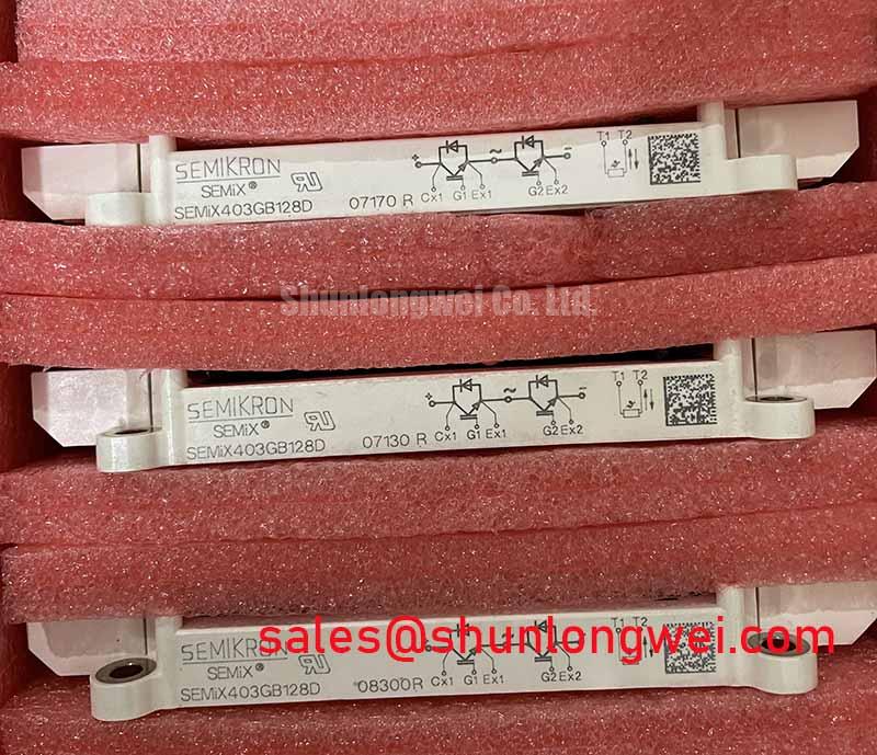
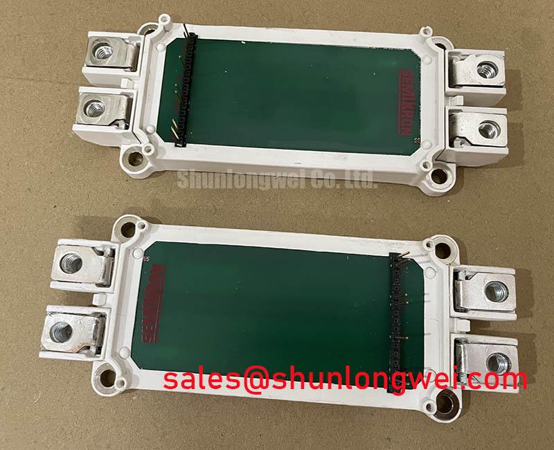
The 1200.0 V and 400.0 A figures are official product ratings supplied for this listing; they do not define the permitted voltage, current, short circuit duration, switching frequency, or overload profile of a complete inverter. Before installation, compare the original circuit topology, gate driver arrangement, protection timing, cooling path, and terminal configuration with the module documentation. The system integrator should verify every gate and emitter connection from the original schematic rather than infer a pin function from a similar package.
Galvanic isolation belongs to the gate driver and the surrounding system unless a specific module document states otherwise. Verify the isolation barrier rating, creepage, clearance, common mode transient immunity, insulation test method, and certification status of the selected driver. Values such as reinforced isolation above 5 kV or CMTI above 100 kV per microsecond must not be attributed to the SEMIX403GB128DS without a supporting manufacturer specification for the complete gate drive arrangement. The practical test is to observe whether the driver maintains the intended gate state during the fastest measured collector emitter transition.
Spurious turn on can be investigated by monitoring the gate to emitter waveform during the opposite switch transition. Check the gate loop inductance, driver return path, Miller current management, isolation power supply behavior, and dead time coordination. If the gate waveform contains an unexpected pulse, that observation may indicate a layout, driver, measurement, or switching interaction; it is not sufficient by itself to identify a failed module. Repeat the measurement with the correct probe reference and compare it against a verified assembly.
Fast semiconductor fuse coordination requires an I2t comparison across the complete fault path. The fuse clearing integral, prospective fault current, DC link capacitance, wiring inductance, and the module’s specified short circuit or surge capability must be assessed together. Do not select a fuse solely from the 400.0 A module rating. The fuse must interrupt the available fault energy within the protection limits documented for the switching device and the converter. A dead short test should only be performed under a controlled laboratory procedure with suitable containment and remote operation.
For background on power semiconductor technology and system level switching challenges, engineers may consult the Wide Bandgap Revolution engineering guide. The technology discussion is complementary and does not change the official ratings or construction of this silicon based product listing. Additional manufacturer information can be reviewed through the Semikron Danfoss Power Electronics and Modules Official Hub.
SEMIX403GB128DS Thermal Interface Evaluation and Mounting Control
Thermal verification should begin with the complete heat path from the semiconductor junction through the module base and thermal interface to the heatsink. The listing identifies the housing as a SEMiX Module, but no baseplate flatness, thermal resistance, mounting pattern, interface material thickness, or permissible case temperature should be invented from the package name. Obtain those values from the applicable mechanical and thermal documentation before preparing the heatsink.
A thin and uniform thermal interface layer is a general design consideration because excessive material, trapped air, contamination, or uneven pressure can increase thermal resistance. A suggested interface thickness range such as 50 to 100 micrometres is not an official parameter for this module unless the manufacturer documentation confirms it. The correct thickness is determined by the selected material, surface finish, flatness, assembly process, and measured thermal behavior.
Clean both mating surfaces using a process compatible with the interface material. Inspect for burrs, particles, damaged threads, and local high spots. Apply the material consistently across the intended contact area and avoid relying on screw pressure to correct substantial heatsink curvature. If a thermal scan shows an unexpected hot region, verify clamping distribution, interface coverage, airflow, coolant conditions where applicable, and temperature sensor placement before concluding that the power module is defective.
Mounting hardware should be tightened in a controlled sequence that distributes pressure gradually across the module. The final torque must come from the Semikron mechanical specification for the exact housing and fastener arrangement. A general M5 industry torque range is not a guaranteed SEMIX403GB128DS value. After installation, inspect the module for mechanical strain and confirm that the power terminals, gate connections, and heatsink remain secure after thermal cycling.
💡 Pro Tip: Disconnect the DC link and verify the stored energy has fallen to a safe level before inserting or removing gate and power connections.
Preventing Spurious Faults During High Voltage and Reliability Evaluation
Altitude, terrestrial neutron exposure, switching transients, and DC link operating voltage can influence power semiconductor reliability, but the SEMIX403GB128DS listing does not provide a FIT rate, Single Event Burnout rate, altitude derating curve, or operating life claim. These values must not be calculated as product facts without a qualified reliability model, test data, environmental assumptions, and an authoritative source such as a manufacturer reliability document or applicable industry guidance.
For equipment installed above 2000 metres, treat reduced air insulation strength as a system design consideration. Recheck terminal creepage, clearance, contamination conditions, enclosure pressure, humidity control, and the applicable safety standard. The module’s 1200.0 V rating does not establish the required external creepage or clearance for a finished inverter. Engineers should verify the physical distances on the assembled busbar, PCB, terminal barriers, and service access points under the actual pollution and altitude conditions.
Neutron induced Single Event Burnout is also dependent on silicon technology, applied electric field, voltage history, current path, exposure environment, and device construction. A numerical FIT estimate requires a defined neutron spectrum and a documented cross section or test basis. Without that evidence, the proper engineering action is to validate voltage headroom through controlled switching and fault tests, inspect repetitive overshoot, and apply a documented system derating policy rather than assigning a universal failure probability.
During commissioning, capture the maximum collector emitter voltage under startup, regeneration, load release, fault interruption, and the highest expected temperature. Compare those measurements with the official device limits and the converter’s protection response. If intermittent trips occur, correlate the event with gate signals, desaturation or overcurrent feedback, DC link behavior, thermal sensors, and isolation power rails. This approach separates a protection coordination issue from a possible power module or wiring problem without making a single symptom prove one cause.
For a neutral comparison during repair planning, engineers may review the separate SKM75GB07E3 product page and verify voltage, current, package, topology, terminal arrangement, thermal data, and gate drive requirements against the original design. Similar appearance or a related product family does not establish interchangeability. The final decision should be based on documented electrical, mechanical, thermal, insulation, and protection compatibility.