



Content last revised on September 17, 2026
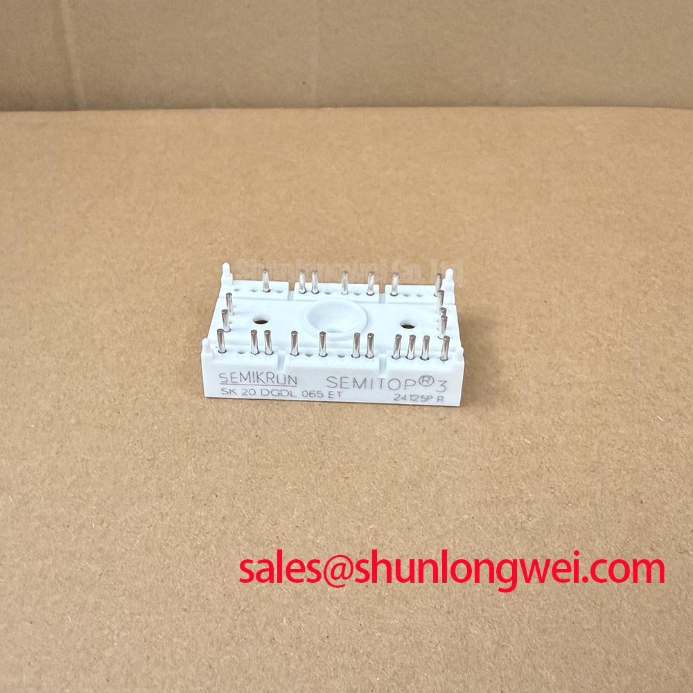
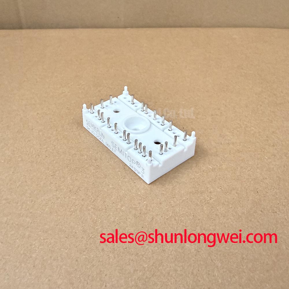
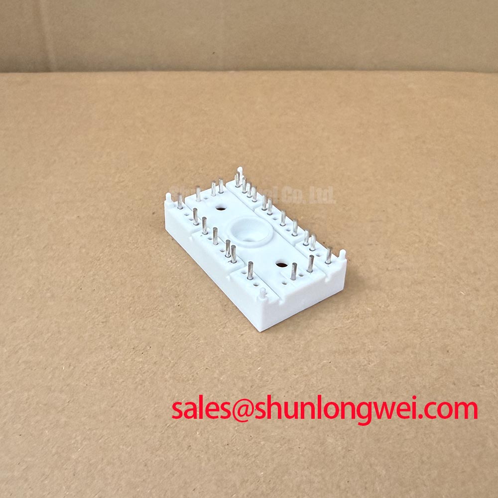
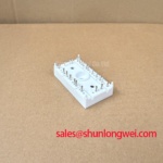
Transient Dynamics and Electrical Design: Evaluating Thermal Capacitance Against the Heat Sink on SK20DGDL065ET
| Model | SK20DGDL065ET |
| Manufacturer | Semikron |
| Category | IGBT Module |
| Topology | Half Bridge Dual IGBT |
| Package | Semitrans |
| Series | Standard |
| Official Specification | Voltage and current ratings are not provided in the supplied official specification set. |
Measure the mounting surface flatness, thermal interface condition, and heat sink contact pattern before attributing a pulsed shutdown to the SK20DGDL065ET. This Semikron Semitrans module is a Half Bridge Dual IGBT assembly, so both switching positions share the same mechanical thermal path but can experience different electrical stress according to the converter commutation sequence.
Thermal capacitance and junction to case transient impedance must be taken from the applicable manufacturer documentation for the exact device revision. Without those official curves, a peak junction temperature margin cannot be calculated responsibly. As a Design Consideration, correlate the load pulse timing with case temperature trend and switching waveform capture. A rapid temperature excursion during repeated pulses can point to degraded heat transfer, excessive switching loss, or an operating point outside the original converter conditions rather than one isolated cause.
Inspect the clamping arrangement for even pressure and remove old compound before assessing contact. Apply a thin, continuous thermal interface layer according to the equipment assembly procedure, then verify that busbars and gate leads are not mechanically loaded by the mounted module. ⚠️ Field Alert: Isolate the DC link and confirm stored energy has discharged before loosening power terminals or disconnecting gate wiring.
For inverter welder and medium frequency induction heating repairs, compare the original pulse pattern with the repaired unit under controlled load. The Semikron Danfoss power electronics hub provides product family context, while the exact device documentation remains the authority for thermal limits and mounting requirements.
Benchtop Waveform Tuning: Checking Isolation Barrier Integrity on SK20DGDL065ET
Check each power terminal against the module baseplate and enclosure ground with approved insulation test equipment at a manufacturer-approved test voltage, and only after disconnecting the surrounding drive circuitry. The supplied official data identifies the package and half bridge topology, but it does not state an isolation test voltage, reinforced insulation classification, or common mode transient immunity figure for SK20DGDL065ET. Those properties must not be inferred from the Semitrans housing alone.
Common mode transient immunity is principally a gate driver and isolation system characteristic. A spurious gate pulse observed at a switching transition can arise from driver isolation behavior, gate return impedance, measurement probe grounding, or capacitive coupling in the physical layout. Use a differential measurement method and compare gate to emitter behavior across both IGBT positions while the DC link and output node transition. Design Consideration: maintain clear separation between high energy power paths and low level driver routing, then validate the result against the converter’s actual switching conditions.
When modules are paralleled in equipment architecture, static current balance cannot be assumed from a module label. Compare controlled, cold state measurements using the same test method, inspect symmetrical conductor paths, and confirm that each gate drive path has equivalent functional behavior. The relationship between on state voltage and temperature can influence sharing, but it does not replace full current and thermal validation. For related power module construction context, see Semikron MiniSKiiP power modules.
💡 Bench Tip: Record diode mode readings and terminal to baseplate insulation observations from a known good assembly before evaluating a suspect module, using ESD controlled handling throughout the test.
Benchtop Waveform Tuning: Assessing Regenerative DC Bus Voltage Surge Dissipation on SK20DGDL065ET
Capture the DC bus waveform during output current reversal or load energy return, then compare the peak and ringing pattern with the original equipment behavior. A half bridge module can participate in power conversion where energy returns to the DC link, yet the supplied official specification does not identify an internal braking IGBT, braking resistor, or energy absorption rating for SK20DGDL065ET.
In inverter welder and induction heating power supplies, a bus surge can involve the input rectifier, DC link capacitors, control response, output load behavior, and any external braking path. Design Consideration: trace the actual energy route on the equipment schematic before replacing power semiconductors. Examine capacitor connections, resistor continuity, braking control signals, and busbar joints; then use oscilloscope measurements to establish whether the observed overshoot follows switching commutation or regenerative loading.
Keep the commutation loop compact to reduce inductive voltage overshoot, while allowing the system engineer to verify peak voltage margins during switching tests. The diode reverse recovery behavior also affects ringing and conducted or radiated noise, but no recovery softness factor is provided for this model in the official data supplied here. Do not assign a numerical recovery characteristic without the applicable device datasheet.
Where a repair requires evaluation of a different physical platform, SEMIX403GB128DS can be reviewed as a separate hardware option. Its terminal layout, ratings, drive conditions, mounting arrangement, and system qualification must be assessed independently; it should not be treated as an automatic replacement.
Assembly Integrity and Layout Architecture: Suppressing Cres Induced Gate Voltage Spikes on SK20DGDL065ET
Probe gate to emitter voltage directly at each device connection while observing the opposite switch transition, because a voltage spike can reveal unintended gate coupling before it becomes destructive cross conduction. In a half bridge, rapid collector voltage movement couples through capacitances associated with the switching structure and the external layout. The resulting gate disturbance depends on driver sink capability, gate loop impedance, common emitter routing, and probe placement.
Design Consideration: use a low impedance turn off path and evaluate an active Miller clamp where the driver architecture supports it, especially when measured gate voltage rises during the opposite switch transition. Any negative gate bias level must be determined from the original gate driver design and the device’s official gate rating; no specific gate bias is established by the supplied specification. Verify dead time, driver supply stability, and gate signal polarity at the connector before declaring the module defective.
Inspect terminal creepage and clearance within the complete assembly, including conductive contamination, loose hardware, damaged insulation hardware, and busbar alignment. These are enclosure level conditions rather than guaranteed properties of the discrete module. For a broader diagnostic framework covering switching stress, gate drive checks, and system reliability decisions, consult the Power Electronics Masterclass. In systems using an associated power stage, the operating relationship of a SKM40GD125D should be verified from the actual schematic and measured waveforms rather than assumed from part category alone.