

Content last revised on October 28, 2026
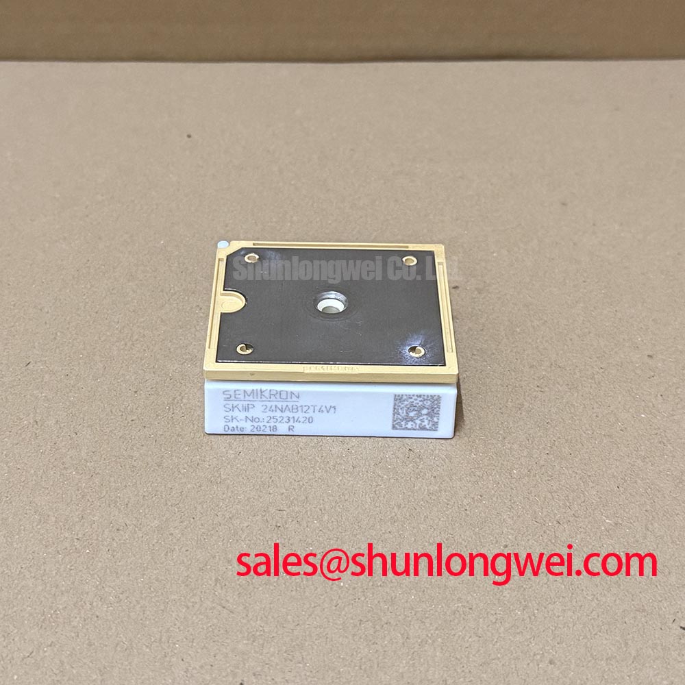
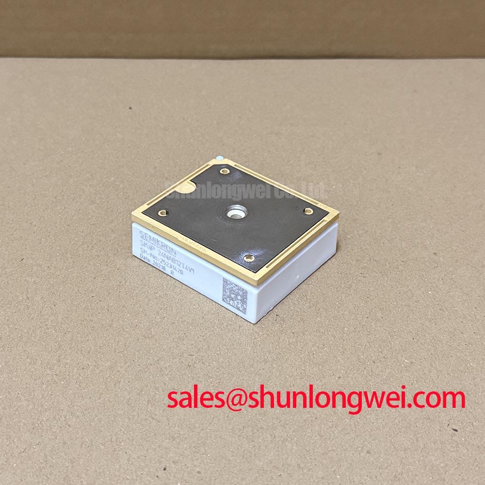
Manufacturer: Semikron | Topology: Converter-Inverter-Brake (CIB/NAB) | Key Rating: 1200.0V, 24.0A (Official Datasheet Specification) | Package Style: MiniSKiiP / SKiiP
SKIIP24NAB12T4V1 Circuit Protection & Reliability: Calibrating Unpowered Bench Screening: Multimeter Diod
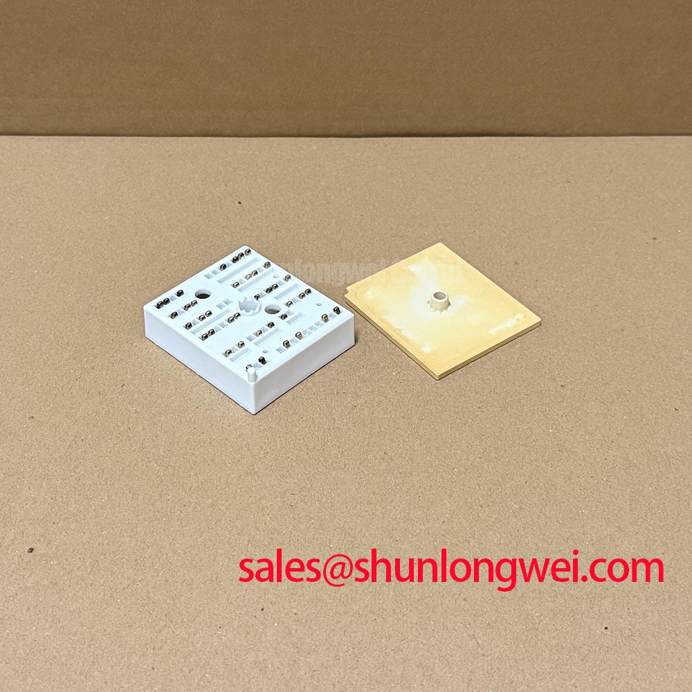
Unpowered bench qualification serves as the first line of defense against catastrophic failure when a drive module arrives in the maintenance workshop from an active plant floor. For an industrial service technician supporting multi-axis motion hardware, taking an out-of-box or field-returned module directly to high-voltage bus energization carries substantial operational risk. The SKIIP24NAB12T4V1 integrates a three-phase input rectifier, a three-phase inverter bridge, and an auxiliary brake chopper within a solderless spring-contact MiniSKiiP platform. Evaluating its internal semiconductor junctions prior to mechanical mounting prevents secondary damage to gate-drive boards, switch-mode auxiliary supplies, and pre-charge resistor networks.
Diagnostic screening begins with a calibrated digital multimeter set to diode-test mode, utilizing an open-circuit test voltage between 2.8V and 3.2V to overcome forward junction thresholds. The measurement targets two distinct semiconductor chemistries within the module: the line-frequency input rectifier diodes and the fast recovery antiparallel freewheeling diodes co-packaged with the IGBT dies. Connect the positive meter lead to the DC negative rail (terminal N) and sweep the negative lead across inverter phase outputs U, V, and W. Each antiparallel diode must present a clean, consistent forward conduction drop. Reversing the test leads across the same terminals must read open-circuit on all channels, confirming that the reverse-blocking capability is intact. Repeat this procedure between the inverter phase outputs U, V, W and the DC positive rail (terminal P) by placing the negative lead on terminal P and probing each phase with the positive lead.
Assessing gate integrity on the 1200.0V IGBT switches requires verifying high gate-to-emitter DC isolation without applying external bias. Using a high-impedance multimeter set to the highest resistance range (megohms), measure between the respective gate spring contacts and their corresponding emitter/Kelvin auxiliary terminals for all six inverter positions and the brake switch. The reading should register well beyond the multimeter's maximum measurable range (over-range / infinite resistance). Any finite resistance reading, such as values descending into kilo-ohms, denotes severe dielectric breakdown across the gate oxide layer, often induced by transient overvoltage or electrostatic discharge during field handling. Reference structural IGBT gate-oxide breakdown phenomena and carrier behaviors in The Ultimate IGBT Knowledge Base for deeper root-cause analysis on dielectric stress mechanisms.
Evaluating the input bridge stage involves probing the input terminals against the internal intermediate rails. The phase-controlled or uncontrolled rectifier stage handles incoming line transients and grid harmonic distortion, where imbalance among phase pairs serves as an early indicator of localized silicon degradation. Forward conduction sweeps from line inputs L1, L2, and L3 toward the positive internal bus bar must demonstrate identical diode drops within narrow production tolerances. Simultaneously, checking the brake chopper branch requires probing between the brake collector terminal and the DC negative rail, testing both the internal freewheeling diode and confirming that the brake IGBT gate is not latched or shorted to the collector. The integrated NTC thermistor contacts must be verified against standard nominal resistance tables at room temperature to ensure temperature tracking circuits receive an accurate feedback signal.
| Test Point Pair | Positive Lead (+) | Negative Lead (-) | Nominal Diagnostic Expectation | Failure Indication & Root Cause |
|---|---|---|---|---|
| Low-Side Inverter Diodes | Negative Rail (N) | Phase Out (U, V, W) | Conduction drop (~0.35V to 0.70V) | 0.00V shorted (die punch-through) or Open (bond wire lift) |
| High-Side Inverter Diodes | Phase Out (U, V, W) | Positive Rail (P) | Conduction drop (~0.35V to 0.70V) | 0.00V shorted or unbalanced forward voltage across phases |
| Inverter Gate Channels | Gate Contact (G1..G6) | Emitter/Kelvin (E1..E6) | High-Z / Open Loop (>50 MΩ) | Measurable resistance indicates gate oxide perforation |
| Three-Phase Input Rectifier | AC Inputs (L1, L2, L3) | Positive Rail (P) | Conduction drop (~0.45V to 0.85V) | Asymmetrical drop indicates line surge / ITSM overstress |
| Internal NTC Sensor | NTC Pin 1 | NTC Pin 2 | Nominal resistance per factory curve | Infinite resistance (cracked substrate or detached solder pad) |
A crucial factor during bench auditing is capacitive charge retention. The internal input capacitance and reverse transfer capacitance ($C_{res}$) across the gate-emitter junction can store minor charges injected by multimeter test currents, creating false conduction states during subsequent high-resistance sweeps. Before taking final leakage readings, short each gate spring terminal to its respective emitter contact momentarily using a grounded, ESD-safe conductive foam pad or a 10 kΩ discharge probe. This step discharges the Miller capacitance, stabilizing the channel and ensuring consistent diagnostic screening prior to mechanical reassembly.
Preventing Spurious Faults: Screening Substrate Ceramic DBC Micro-Crac Guidelines for SKIIP24NAB12T4V1
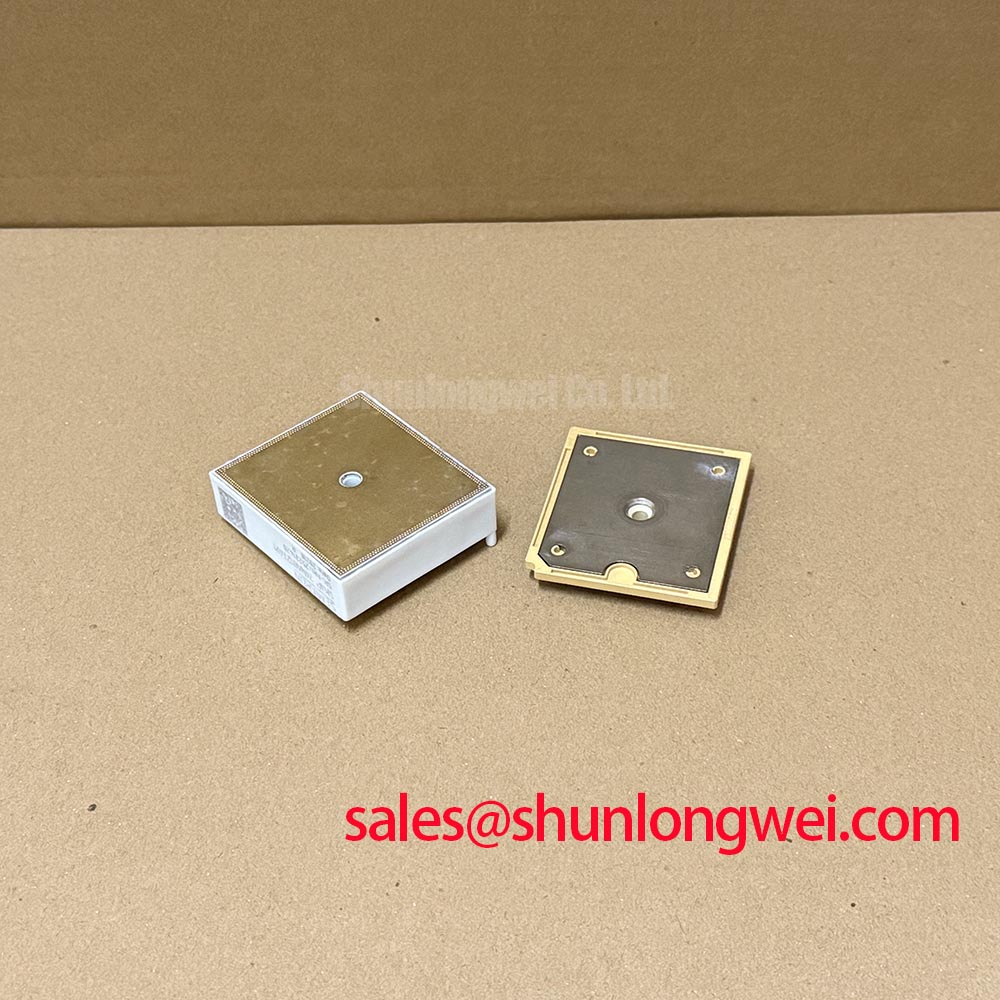
Power cycling in demanding factory automation settings places severe thermal and mechanical stresses on the internal layers of power modules. The SKIIP24NAB12T4V1 leverages a baseplateless Direct Copper Bonded (DCB) ceramic architecture utilizing pressure-contact technology, characteristic of the Semikron MiniSKiiP® Power Modules series. Because the module does not possess a thick copper baseplate, the aluminum oxide ($Al_2O_3$) ceramic substrate sits in direct thermal contact with the external aluminum heatsink. This structure provides low thermal resistance, but it demands strict assembly tolerances to prevent mechanical stresses that could cause micro-fissures in the ceramic substrate.
Substrate micro-cracks compromise dielectric isolation between the 1200.0V DC bus tracks and the grounded heatsink chassis. Under industrial plant conditions where airborne conductive particulates, cutting fluid aerosols, and ambient humidity accumulate, a hairline fissure creates an ionization path that results in intermittent ground fault trips or catastrophic substrate breakdown. Verifying isolation integrity requires high-voltage insulation testing across the power terminals and the thermal interface plane. Apply a DC test voltage of 2.5 kV between all shorted power terminals (P, N, U, V, W, L1, L2, L3) and the module’s mounting footprint or grounded heatsink. The isolation resistance should comfortably exceed 500 MΩ under clean bench conditions. Any dynamic instability in insulation resistance during voltage ramp-up warns of partial discharge activity across localized ceramic micro-fractures.
Preventing substrate fractures centers primarily on proper mounting torque execution and controlled thermal interface material (TIM) application. The heatsink surface profile must comply with standard machining flatness guidelines: a localized surface roughness ($R_z$) of 6.3 µm or better, and a planarity deviation of less than 20 µm across the module contact area. If the heatsink exhibits a concave or convex curvature outside these limits, tightening the central clamping screw forces the brittle ceramic substrate to bend, initiating micro-cracks along etched copper borders.
TIM thickness optimization plays an equally critical role in structural survival and heat dissipation. Apply non-silicone or phase-change thermal paste with a wet layer thickness controlled strictly between 50 µm and 80 µm, preferably utilizing a precision screen or patterned roller. Excessive thermal compound acts as a hydraulic wedge during screw down; because grease is an incompressible fluid, tightening the module against a heavy grease pool creates concentrated tensile stresses in the center of the DCB ceramic. Conversely, insufficient compound creates localized thermal insulation voids, driving operational junction temperatures past silicon limits during robotic motor acceleration bursts.
⚠️ Maintenance Note: Periodically monitor heatsink terminal temperature delta under full plant load using thermal imaging, and schedule a physical air-duct blowout every six months to prevent dust cakes from bridging external creeping clearances across pressure-contact spring housings.
When torqueing the central mounting screw of the MiniSKiiP housing, observe a calibrated tightening sequence using an adjustable torque screwdriver. Industry assembly guidelines specify bringing the fastener to a soft seating snug, followed by continuous tightening to the target torque—typically 2.0 to 2.5 N·m (Design Consideration for standard MiniSKiiP clamping assemblies). Fastener over-tightening or using non-calibrated electric drivers subjects the pressure-