Content last revised on September 19, 2026
T930S18TOF Operational Boundaries: Evaluating Critical Rate of Rise of Off-State Voltage Limits
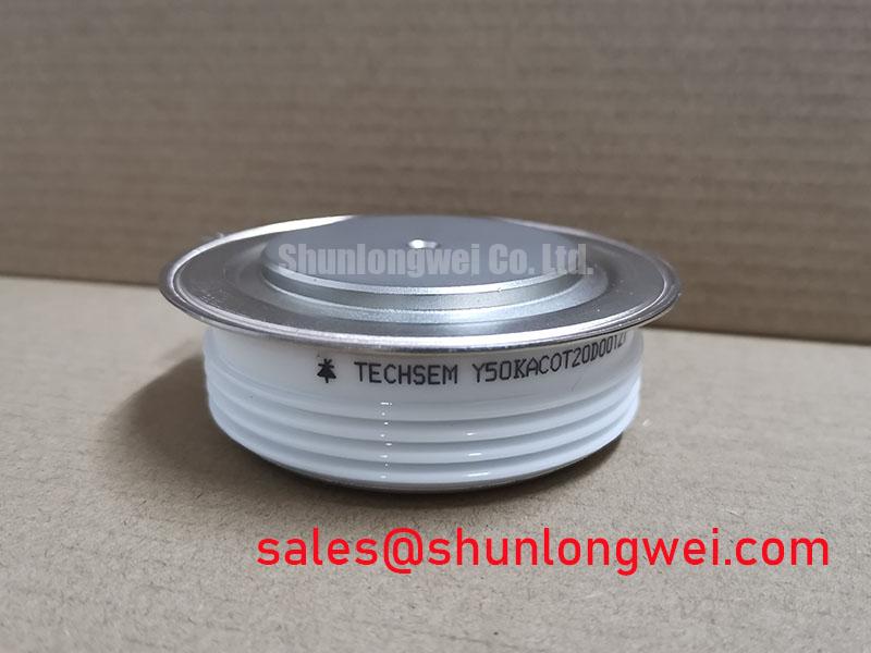
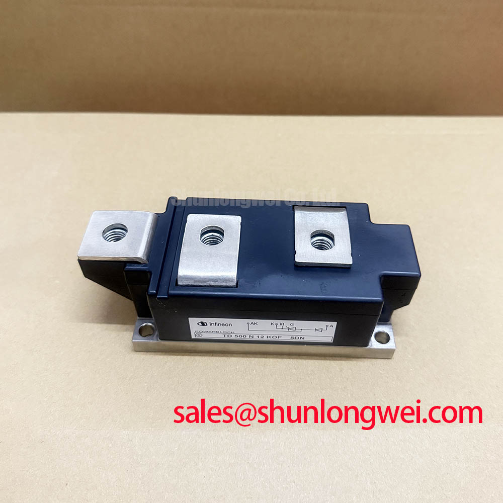
| Model | T930S18TOF |
| Manufacturer | Infineon |
| Product Category | Thyristor/Diode Module |
| Package | PowerBlock Module |
| Rated Voltage | 1800 V Official Specification |
| Rated Current | 930 A Official Specification |
Capture the anode to cathode voltage waveform across the installed T930S18TOF during each commutation event, with the probe reference connected at the device terminals rather than at a remote cabinet ground. Ringing observed at the PowerBlock terminals can reveal a layout induced voltage transition that differs substantially from the waveform measured at the DC link.
The 1800 V rating is an Official Specification and establishes the voltage boundary for this Infineon thyristor/diode module. It does not, by itself, define an acceptable system switching waveform, snubber value, reactor saturation point, or repetitive transient condition. Engineers assessing a medium frequency induction melting or hardening furnace should compare the measured off state voltage, transient overshoot, and rate of voltage rise with the applicable device documentation and the original converter design requirements.
RC snubbers are commonly evaluated as a Design Consideration where rapid voltage transitions can couple through device capacitances and trigger unintended conduction. Their effectiveness depends on the complete commutation loop, including busbar geometry, capacitor placement, transformer leakage inductance, load condition, and the behavior of the associated diode path. A snubber that removes visible ringing at one operating point can create additional dissipation or alter commutation behavior at another point, so final component selection belongs to system level testing.
Series saturable reactors can also be examined where the converter requires controlled current rise during turn on. Their purpose is not to compensate for an unknown device limit. Instead, they are evaluated with the actual pulse current, magnetic reset condition, and mechanical installation arrangement to reduce localized current concentration during stressful switching intervals.
Inspect terminal joints for uneven contact pressure, heat discoloration, loosened hardware, and copper interfaces that have shifted under thermal cycling. The module terminal arrangement and connection sequence must follow the converter drawing and device documentation. A loose or asymmetric current path may increase stray inductance and produce waveforms that do not represent the intended circuit behavior.
💡 Pro Tip: Keep positive and negative commutation conductors physically coupled and verify turn off voltage peaks with a properly rated differential probe at the module terminals.
For repair planning, the TT500N18KOF can be reviewed as a separate compatible device candidate only after engineers have verified topology, terminal arrangement, voltage class, current duty, cooling interface, and firing requirements against the original assembly.
T930S18TOF Operational Boundaries: Evaluating Reverse Recovery Charge Limits
Measure commutation current and device voltage together while the furnace supply moves through its real load range, then inspect the transition for reverse recovery current peaks, recovery softness, and voltage oscillation. A current probe on the diode path and a differential voltage probe across the module provide more useful evidence than relying on cabinet level voltage alone.
The T930S18TOF is rated at 1800 V and 930 A as Official Specifications. Reverse recovery peak current, recovery time, reverse recovery charge, and waveform softness are separate device characteristics that must be taken from the applicable original product data and evaluated under the converter’s actual current slope, junction temperature, and commutation network. They must not be inferred from the module current rating.
In a medium frequency induction power supply, diode recovery behavior can influence thyristor turn off stress, commutation loss, and radiated noise. A sharp recovery current transition may interact with busbar inductance and DC link capacitance, while a slower transition can redistribute loss into another part of the commutation interval. These are Design Considerations, not factory performance claims for this specific module.
Review the DC link capacitor connections and the physical distance between the capacitor bank, module terminals, and commutation conductors. The objective is to minimize parasitic loop inductance where it contributes to voltage overshoot and ringing, then verify peak voltage margins during switching tests. Busbars with unequal paths can also cause current sharing differences between parallel circuit sections.
The input supply section deserves equal attention when the converter includes separate controlled rectification hardware. For example, the SKKT500/14E is a thyristor module that may appear in related rectifier topologies, but its role, firing arrangement, and ratings require an independent engineering check rather than an assumed substitution relationship.
Where recovery related interference is suspected, isolate the event by comparing waveforms before and after checking gate command timing, commutation capacitor condition, conductor symmetry, and measurement probe placement. A changed waveform may indicate several interacting causes, including an altered load, a degraded passive component, timing variation, or an impedance mismatch in the power path.
T930S18TOF Thermal-Electrical Optimization: Preventing Localized Gate Hotspot Burnout Practical Tuning
Probe the gate to cathode firing waveform directly at the relevant control terminals and compare pulse shape, timing consistency, and pulse persistence across repeated converter cycles. A gate pulse that looks satisfactory at the driver board can become distorted at the module because of cable inductance, return path impedance, connector condition, and electromagnetic coupling from the main current loop.
Gate firing characteristics, gate current rise, holding behavior, and permissible repetitive pulse conditions are not established by the supplied 1800 V and 930 A ratings. They must be confirmed from the correct Infineon product documentation for the installed device and tested against the original firing circuit. Do not apply a generic gate current threshold, negative bias level, or pulse duration as though it were an official requirement for T930S18TOF.
Design Consideration: a low inductance gate loop with a closely paired gate and return conductor helps preserve the intended firing pulse at the module terminals. This matters where main circuit voltage transitions can couple into the gate circuit and disturb the intended firing instant. The firing transformer, isolation barrier, return routing, and suppression network should be examined as one path rather than as independent parts.
For systems using isolated gate drive control, engineers can review the isolation and signal integrity concepts discussed in Infineon EiceDRIVER™ galvanic isolated gate driver ICs. The driver family information supports gate drive architecture review, while the final gate network remains dependent on the installed module, converter topology, and measured switching conditions.
Multi pulse firing can be evaluated when the original converter strategy uses repeated gate commands to maintain dependable triggering under varying load and commutation conditions. It should be checked against the firing transformer’s reset behavior, control timing, and device gate limits. Changes to pulse scheduling without verifying the main circuit waveform can shift heat and current stress into less visible operating intervals.
Thermal inspection should focus on the external thermal interface, clamping uniformity, heatsink flatness, airflow or liquid cooling performance, and evidence of uneven temperature distribution around the PowerBlock footprint. The module package is a mechanical and electrical interface; a localized thermal pattern may reflect cooling contact variation, current path imbalance, or abnormal commutation energy rather than a single device level cause.
Assembly Integrity & Layout Architecture: Implementing Fuse Total Clearing I2t versus Semiconductor Withstand I2t for T930S18TOF
Compare the semiconductor fuse total clearing I2t curve with the fault current waveform and the device withstand data used by the original protection design before returning the converter to service. The decisive comparison is the energy passed by the fuse through the actual fault path, including pre arcing and clearing behavior, rather than the fuse current label alone.
The supplied official information identifies T930S18TOF as a 1800 V, 930 A Infineon PowerBlock thyristor/diode module. No device withstand I2t value, fuse coordination table, mounting torque, or terminal torque is included in the provided official specification set. These values must therefore not be assigned as factory parameters. The original module documentation, fuse documentation, and converter protection drawing establish the data needed for a valid coordination review.
Engineering Calculation may be used when complete verified data is available: the protection engineer compares the fuse total clearing I2t under the anticipated prospective fault current with the relevant semiconductor surge or withstand boundary, while accounting for the complete current path. The result must also consider contact resistance, conductor cross section, source impedance, DC link energy, and whether parallel paths alter fault current distribution.
Fuse placement is a Design Consideration involving the physical fault loop as well as electrical coordination. A fuse positioned so that substantial stored energy remains downstream may not control all of the energy delivered into a short circuit. Likewise, long unconstrained conductors can add inductive stress even when the fuse interrupts correctly. Verify the installed layout against the machine schematic, protective earth arrangement, enclosure clearances, and service isolation procedure.
After a fault event, inspect the module terminals, busbars, fuse holders, commutation capacitors, firing connectors, and heatsink contact areas before fitting a replacement. Check for shifted conductors, damaged insulation, loosened fasteners, and changes in circuit continuity with power removed. The Field Engineer’s Handbook provides additional measurement focused guidance for structured failure analysis and preventive inspection.
When integrating this module into an induction melting or hardening furnace supply, engineers should verify the full fault interruption sequence under controlled conditions, including command inhibit behavior, fuse response, contactor or breaker coordination, and discharge of stored energy. Protection performance is determined by the complete power system, not by the module voltage and current rating alone.