




Content last revised on October 27, 2026
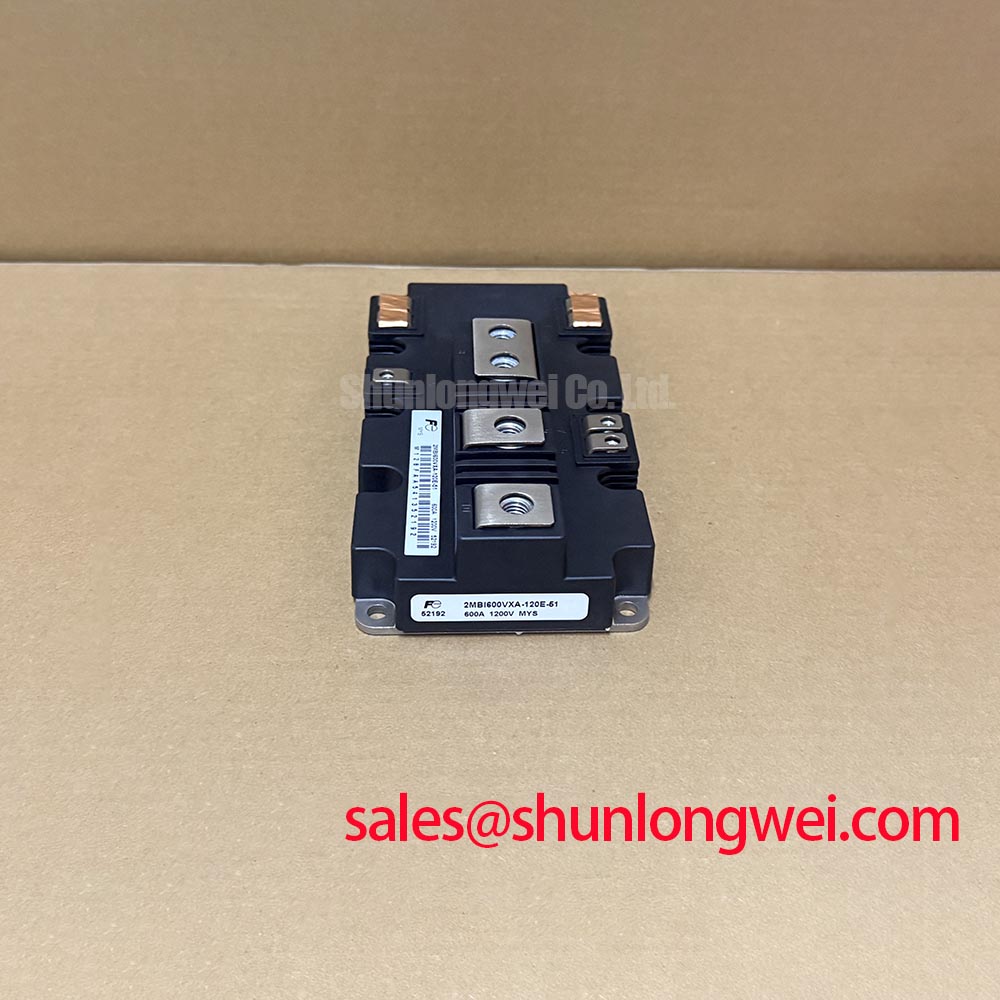
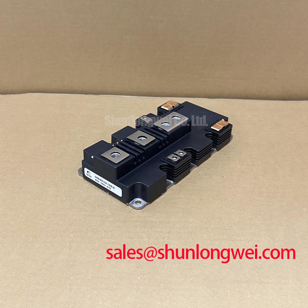
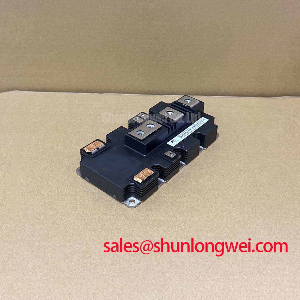
2MBI600VXA-120E-51 Fuji Electric 1200V 600A IGBT Module
Before inspecting a traction inverter cabinet that has reported a regenerative braking or DC bus fault, isolate all energy sources and verify that the DC link has discharged according to the equipment’s safety procedure. Inspect the module terminals and mounting interface before re-energizing. The device identified for this position is the Fuji Electric 2MBI600VXA-120E-51, a 1200 V, 600 A IGBT module in a Fuji Power Module package.
Its factory-defined topology is a 2-in-1 half-bridge IGBT from Fuji Electric’s 6th Gen V-Series. These ratings establish the component identity; they do not replace the system engineer’s checks for switching waveform stress, cooling capacity, gate-drive compatibility, insulation coordination, or regenerative energy management. The 600 A rating applies under the datasheet’s specified conditions, not as an unconditional continuous operating current.
| Parameter | Factory specification |
|---|---|
| Manufacturer | Fuji Electric |
| Part number | 2MBI600VXA-120E-51 |
| Category | IGBT Module |
| Series | 6th Gen V-Series |
| Topology | 2-in-1 Half-Bridge IGBT |
| Voltage rating | 1200 V VCES |
| Current rating | 600 A IC under the specified datasheet conditions |
| Package | Fuji Power Module |
Assembly Integrity & Layout Architecture: Implementing Baseplate Convexity Inspection for 2MBI600VXA-120E-51
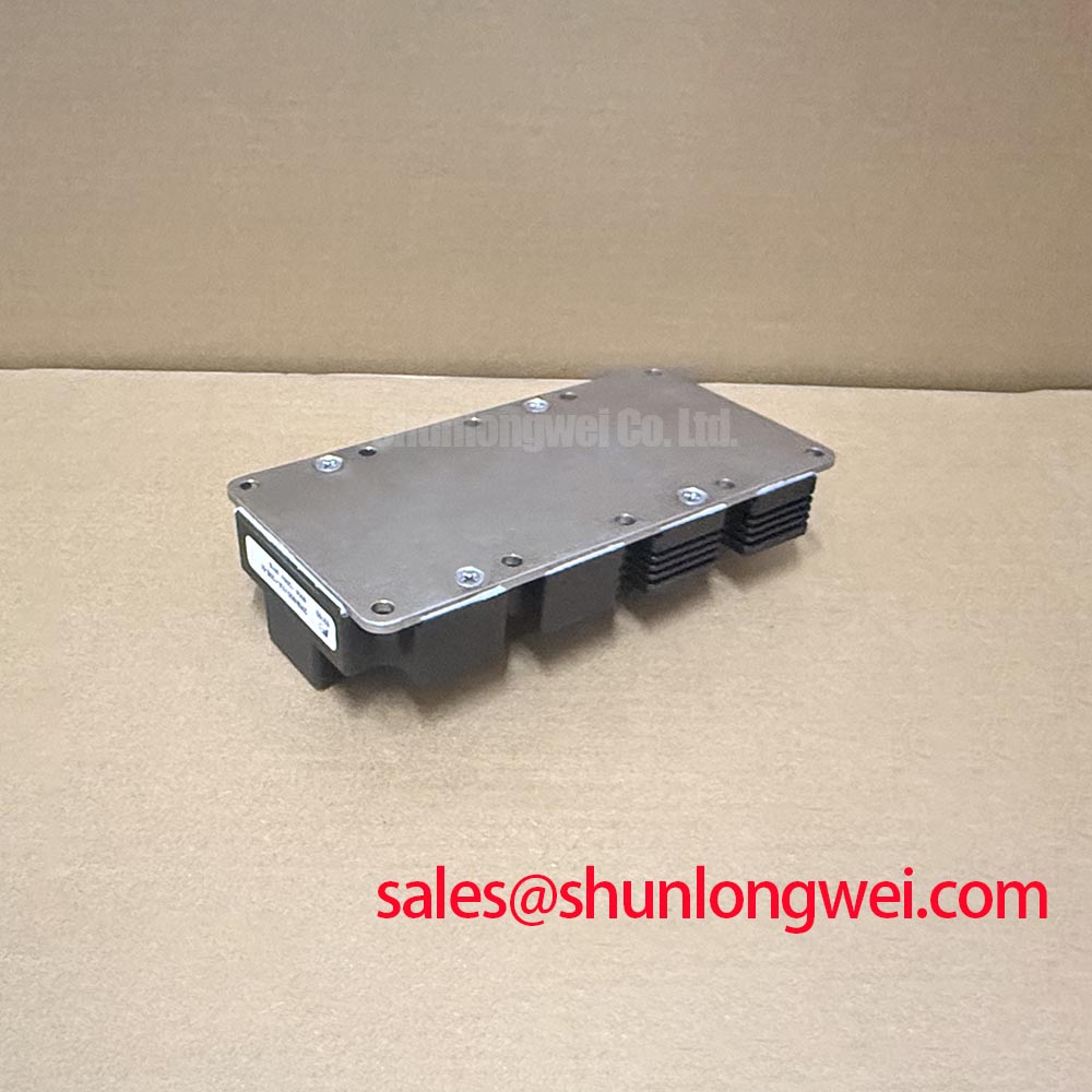
Inspect the module baseplate and heatsink contact surfaces before applying thermal interface material. Baseplate deformation outside the manufacturer’s permitted tolerances, contamination, burrs, or a locally damaged heatsink can produce uneven contact pressure. Specified baseplate convexity should not itself be treated as a defect. The resulting thermal path may remain electrically functional during a cold test while creating excessive junction temperature during sustained traction or braking duty.
Use a calibrated flatness inspection method appropriate to the maintenance workshop, then record high spots, surface damage, and the condition of the mounting holes. The heatsink should be clean, stable, and free from raised particles. Thermal interface material should be applied as a controlled, continuous layer according to the selected material supplier’s process. The practical objective is uniform coverage without voids, excessive squeeze-out, or mechanical stress transferred into the module substrate.
Position the module so that the power terminals, gate-drive connections, and DC-link conductors can be routed without forced bending. Keep the commutation loop compact and arrange the two half-bridge current paths symmetrically where the cabinet topology allows. Mechanical alignment should be completed before final tightening; using the fasteners to pull a misaligned module into position can distort the baseplate and compromise long-term thermal contact.
Apply the tightening sequence specified by the equipment or module documentation, using a calibrated tool and a diagonal cross-pattern where specified. Recheck that the baseplate remains seated after the first controlled pass. A gradual sequence is preferable to tightening one corner fully before the others because it distributes pressure across the mounting surface and reduces the chance of substrate stress.
Maintenance Note: Record heatsink temperature rise during scheduled service and inspect fan paths, filters, and thermal interface condition whenever the trend changes.
For a repair evaluation involving another Fuji module, the 2MBI25L-120 may be reviewed as a separate device, but voltage class, current capability, terminal arrangement, gate characteristics, mechanical dimensions, and protection settings must be compared before any substitution decision.
2MBI600VXA-120E-51 Thermal-Electrical Optimization: Planar Symmetrical Busbar Geometry
Route the DC-link and switching conductors as a controlled commutation structure rather than as ordinary cabinet wiring. Stray inductance converts rapid current change into collector-emitter overshoot, so the busbar should place opposing current paths close together and avoid unnecessary conductor loops. The appropriate geometry is determined by the complete inverter layout, switching speed, DC-link capacitor position, and measured waveform.
During commissioning, verify every power terminal against the equipment schematic before connecting the gate-drive board. A 2-in-1 half-bridge topology requires correct identification of the upper switch, lower switch, midpoint, and DC-link connections. Do not rely on terminal appearance alone when a replacement module is being evaluated. Confirm the gate and emitter connections using the applicable Fuji documentation and the original drive-board pin mapping.
Oscilloscope probing should use suitably voltage-rated differential or isolated probes and a measurement arrangement that minimizes probe-loop pickup. Compare the collector-emitter waveform at the module terminals with the gate-emitter waveform at the module pins, not only at the remote driver output. This distinction helps separate gate-loop ringing from power-loop overshoot and prevents a busbar issue from being incorrectly corrected with excessive gate resistance.
Snubber selection belongs to the complete switching network. Its capacitance, damping, pulse-current capability, mounting position, and dielectric voltage rating should be selected from measured transient energy and the required clamping boundary. The switching relationship between DC-link voltage, parasitic inductance, and current slew explains why a compact planar busbar can reduce overshoot, but the final margin must be demonstrated under the highest relevant load and temperature condition.
Fastening hardware should resist vibration without allowing the laminated conductors to shift. Inspect contact pressure, washer condition, insulating barriers, creepage paths, and clearance around the highest-potential conductors after the cabinet has completed its vibration or transport procedure. Do not place control wiring across the switching-current path where capacitive coupling can inject disturbance into the gate driver.
Fuji Electric’s power semiconductor reference material provides useful background for understanding switching-device behavior, while the final busbar and gate-drive design remains specific to the converter platform and its test conditions.
Benchtop Waveform Tuning: Mitigating Stress via Regenerative DC-Bus Voltage Surge Dissipation
Start regenerative braking tests with the DC-link energy path clearly identified. When a motor decelerates, mechanical energy can raise the DC-link voltage faster than the converter can return energy to the supply. The braking chopper, ballast resistor, DC-link capacitor, control threshold, and switching device must therefore be evaluated as one energy-management system.
The 2MBI600VXA-120E-51 provides the specified IGBT module identity and rating for the evaluated power stage, but it does not by itself define the braking resistor value, pulse duration, duty cycle, or allowable DC-link surge. Those values depend on motor inertia, speed, deceleration profile, line regeneration capability, capacitor condition, ambient temperature, and the protective trip threshold.
On the bench, monitor DC-link voltage, chopper gate command, collector-emitter voltage, braking-resistor current, and heatsink temperature in the same test record. A chopper that activates correctly may still experience excessive switching stress if the resistor wiring is long, the local capacitor is degraded, or the clamp response is delayed. The waveform should be checked during both the first braking event and repeated braking cycles because resistor thermal loading can change the operating point.
High-power ballast resistors require clear separation from temperature-sensitive control wiring and adequate enclosure airflow. The resistor’s pulse-energy capability should be matched to the deceleration event rather than selected only from continuous wattage. The braking IGBT and its protection circuit also require coordination with the fast semiconductor fuse, gate shutdown path, and DC-link discharge procedure.
Where an isolated gate driver or optocoupler is used, examine common-mode transient behavior at the actual module terminals. A driver that appears stable during low-voltage testing may show false pulses when the power stage produces a rapid common-mode transition. Adjusting the gate loop, isolation layout, and return-current path should follow measured waveforms and the driver manufacturer’s specified operating limits.
High-frequency charging and discharging of bootstrap capacitors, where used by the selected gate-drive architecture, should be checked against driver supply-current demand and diode recovery behavior. The system integrator should verify that the capacitor retains adequate gate-drive voltage throughout the intended switching sequence rather than assuming that a nominal auxiliary supply will remain stable under all regenerative events.
2MBI600VXA-120E-51 Circuit Protection & Reliability: Calibrating Thermal Feedback
Use thermal feedback to distinguish a controlled overload response from an abnormal switching condition. Collector-emitter saturation voltage can vary with current and temperature, and a positive temperature coefficient, in the operating region where it applies, can support static current-sharing analysis when devices operate in a properly matched and symmetrical circuit. It should not be treated as a universal substitute for a dedicated temperature sensor or a complete protection strategy.
For parallel power paths, keep gate-loop lengths, driver impedance, emitter returns, and control references as symmetrical as the physical layout permits. The dynamic balance depends on parasitic inductance and mutual coupling as much as on nominal component values. Measure the gate-emitter voltage directly at each module position during turn-on and turn-off to identify unequal drive amplitude, ringing, or delayed transition.
Protection coordination should include desaturation or overcurrent detection where supported by the driver design, controlled gate shutdown, DC-link overvoltage monitoring, and a correctly selected semiconductor fuse. The fuse’s I²t coordination must be evaluated against the converter’s short-circuit response time and the module’s permitted fault behavior; a fuse is not a substitute for sufficiently fast electronic IGBT protection. A fuse that opens too slowly can allow destructive energy to accumulate, while an unsuitable fast fuse can create nuisance interruptions during legitimate current transients.
Freewheeling diode behavior also affects electromagnetic performance. Reverse-recovery softness, commutation-loop inductance, junction temperature, and gate timing influence the amplitude and spectral content of the transient. When radiated or conducted interference changes after a module replacement, compare the diode current and voltage waveforms with the known-good assembly before modifying shielding or filtering.
During preventive maintenance, inspect terminal discoloration, loosened busbar joints, fan performance, condensation traces, and evidence of thermal cycling around the mounting interface. High-speed rail and heavy freight locomotive traction inverters may be considered among the demanding applications for this class of module, but the actual suitability assessment must include the vehicle converter topology, cooling architecture, insulation system, vibration environment, and validated protection thresholds. For broader implementation guidance, see IGBT Design & Integration.