

Content last revised on September 21, 2026
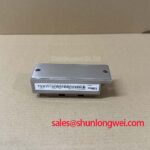
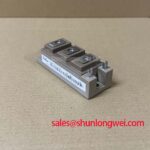
Transient Dynamics & Electrical Design: Galvanic Gate Drive Isolation, Reinforced on 2MBI75VA120-50
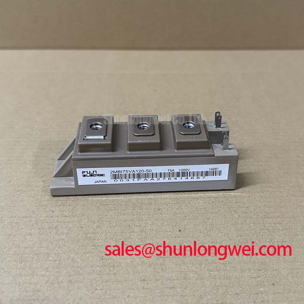
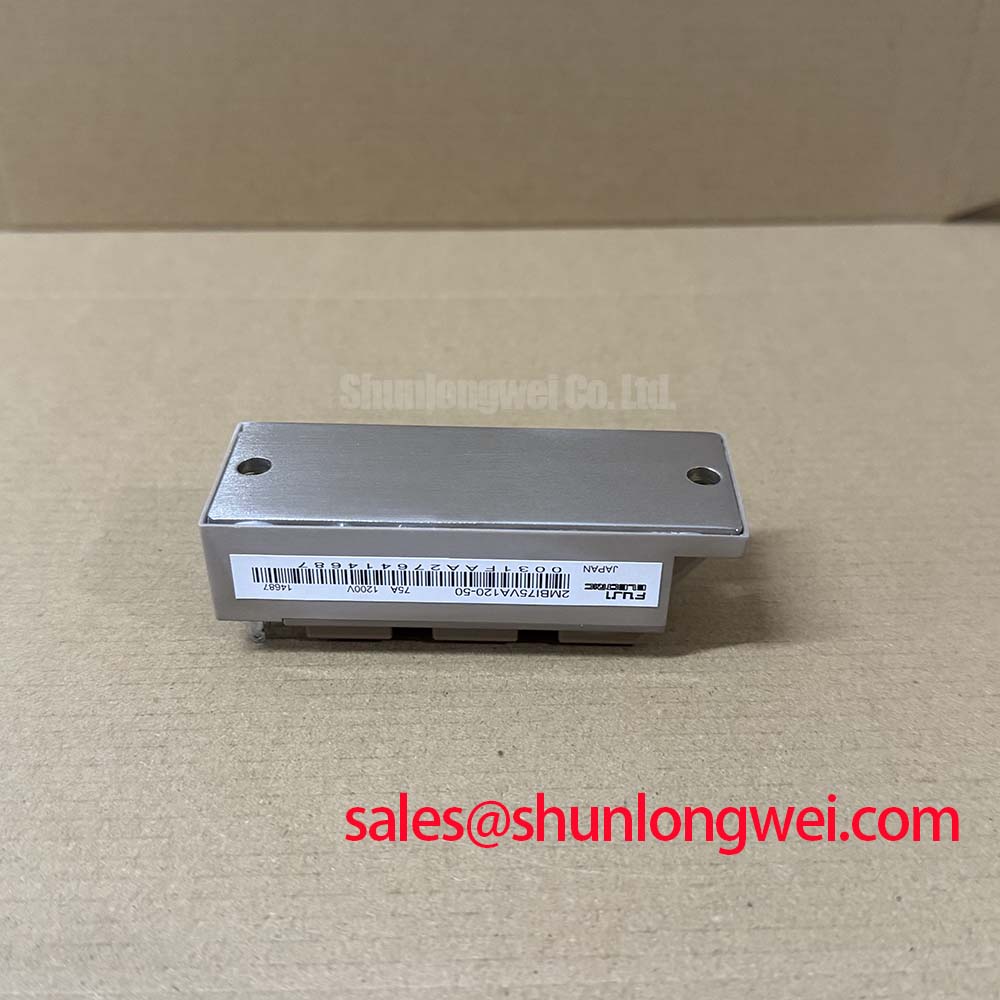
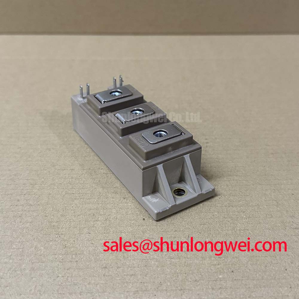
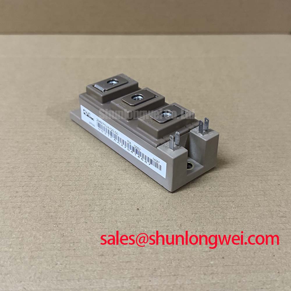
Before reconnecting a stopped inverter, isolate the DC link and compare the cold-state resistance readings between the main power terminals and each gate terminal against the removed module and the equipment schematic. The 2MBI75VA120-50 is a Fuji Electric IGBT module rated at VCES = 1200V and IC = 75A at TC = 80°C, according to the official specification. Its gate-emitter limit is VGES = ±20V; a gate-drive supply, probe reference, or insulation fault must never be allowed to push the actual gate-emitter voltage beyond that boundary.
For a traction inverter or material-handling drive repair, the gate driver needs to be assessed as part of the installed power stage rather than as a separate board. A galvanically isolated driver barrier separates the low-voltage controller reference from switching-node movement. Design Consideration: the drive isolation system should be selected and verified for the converter’s measured common-mode voltage transient, insulation coordination requirements, PCB creepage arrangement, connector spacing, and operating environment. The module’s official VISO = 2500V AC for 1 minute is a module isolation specification; it does not independently establish the isolation performance of the gate-driver transformer, isolated supply, optocoupler, digital isolator, or completed inverter assembly.
During a field inspection, scope the gate-emitter waveform directly at the relevant module terminals with an appropriate isolated or differential measurement method. Compare the command signal, actual gate voltage, collector-emitter switching waveform, and fault input timing. A gate waveform that changes when the opposite device commutates may indicate a shared return path, poor driver referencing, excessive coupling, or probe-induced measurement error. It should be investigated against a known-good channel before replacing power hardware.
The official threshold range is VGE(th) = 6.0V minimum to 7.0V maximum, specified at VCE = 20V and IC = 72mA. This threshold test condition is not an operating gate-drive recommendation and must not be treated as the voltage required to carry the inverter load current. The original driver documentation and switching test results remain the correct references for gate-drive amplitude, turn-off bias strategy, desaturation protection, and dead-time control.
Where a fault is suspected after a module replacement, inspect the gate connectors, driver supply rails, return paths, isolation slots, and gate resistor locations before applying full bus voltage. Fuji Electric’s power semiconductor technical information is also a useful manufacturer resource when reviewing the broader behavior of power switching devices and associated drive arrangements.
Preventing Spurious Faults: High-Frequency Commutation Loop Inductance Guidelines for 2MBI75VA120-50
The main terminals, DC-link capacitors, busbars, snubber parts, and output connections should be inspected as one commutation path before assigning a shutdown event to the 2MBI75VA120-50. At turn-off, peak collector-emitter voltage is influenced by the DC-link voltage plus the product of stray loop inductance and current-change rate. This is an Engineering Calculation principle, not a fixed module-level operating value. It explains why a mechanically sound replacement can still experience abnormal switching stress if the original laminated busbar, capacitor placement, or terminal routing has been disturbed.
Design Consideration: minimize the area enclosed by the high-current commutation loop so that inductive overshoot and ringing are reduced. In service work, look for displaced DC-link capacitors, loosened busbar interfaces, uneven terminal seating, long temporary test leads, or substituted cable paths. These conditions can alter switching behavior even when static multimeter checks show no obvious short circuit. Oscilloscope verification should compare peak collector-emitter voltage and ringing against the system’s specified operating boundary during controlled switching tests.
RC snubbers, MOV protection parts, and DC-link capacitors must be evaluated by their original circuit role. An MOV can contribute to coordinated overvoltage absorption at a defined point in a system, but it does not correct excessive commutation inductance. An RC network can suppress selected ringing modes, yet its suitability depends on measured frequency content, capacitor voltage rating, resistor pulse capability, thermal conditions, and the original drive topology. Engineering Recommendation: retain the original protection network configuration unless the inverter designer has confirmed a revised design through measurement.
Dead-time behavior requires the same restraint. The driver must prevent cross-conduction between switching devices while preserving the intended current-control performance. Excessively short dead time may allow overlap during switching transitions; excessive dead time may distort phase current and increase diode conduction. The required setting is system-determined and should be verified with the installed driver, PWM controller, current sensor, DC-link voltage, and load conditions. Do not infer it from the IGBT’s current rating alone.
For repair situations where the existing mounting pattern, electrical topology, and ratings need to be compared with another Fuji Electric module, the 2MBI300U4H-120-50 can be reviewed as a separate technical reference. Its mechanical outline, terminal arrangement, gate-drive requirements, electrical ratings, thermal path, and protection settings must be verified against the original equipment documentation before any substitution decision.
In systems using separate rectifier and inverter functions, the condition of upstream conversion hardware also affects DC-link ripple and fault behavior. The 2MBI400TB-060-01 is relevant for objective comparison where that type of complementary power-stage device is present in the same equipment architecture. It should not be treated as an automatic replacement for this 1200V, 75A IGBT module.
2MBI75VA120-50 Thermal-Electrical Optimization: Thermal Paste Degradation Prevention and Practical Tuning
Remove the module only after confirming that stored DC-link energy has been discharged according to the equipment procedure, then inspect the contact surface, mounting hardware, heatsink flatness, and residue pattern left by the thermal interface material. The official maximum junction temperature of the 2MBI75VA120-50 is Tj = 175°C. This is a semiconductor temperature limit, not a target for routine operation or a direct indication of heatsink temperature.
Official thermal resistance values are Rth(j-c) = 0.32°C/W for the IGBT and Rth(j-c) = 0.53°C/W for the FWD. These values describe junction-to-case thermal paths under specified manufacturer conditions. Actual junction temperature in a forklift traction controller also depends on switching loss, conduction loss, current waveform, PWM strategy, ambient temperature, heatsink thermal resistance, airflow, interface condition, duty cycle, and the cooling system’s service condition.
Design Consideration: apply compatible thermal interface material as a continuous, controlled thin film, avoiding dry regions, trapped debris, and excessive accumulation around mounting points. Paste condition matters because an aged, displaced, or contaminated interface can raise the temperature drop between the module case and heatsink. A print pattern that is uneven after removal may indicate that mounting pressure, heatsink flatness, surface cleanliness, or application method deserves attention. It does not by itself identify one definite failure cause.
Install mounting fasteners in a gradual alternating sequence so the module seats evenly on the heatsink. Use the equipment manufacturer’s specified screw size, torque procedure, and tightening order rather than applying a generic value. Where spring washers or disc-spring hardware form part of the original clamping assembly, retain their orientation and arrangement because their function is tied to the mechanical stack-up used by the equipment manufacturer.
⚠️ Field Alert: Do not energize a newly mounted module until excess thermal compound is cleared from terminals and the complete gate-drive connection has been rechecked with power removed.
The typical collector-emitter saturation voltage is VCE(sat) = 2.15V at IC = 75A and Tj = 125°C. This official typical value is useful for loss assessment under its stated condition, but it is not a fixed field measurement target. A significant difference in measured operating temperature between inverter phases may arise from load imbalance, sensor position, cooling obstruction, control behavior, switching conditions, interface quality, or device condition. Check these factors methodically.
2MBI75VA120-50 Circuit Protection & Reliability: Evaluating Thermal Transients and Heat-Sink Temperature
When an inverter trips during lifting, acceleration, regenerative braking, or repeated direction changes, record the controller fault code, DC-link voltage, current command, actual phase current, heatsink temperature, and gate-drive fault response before removing the module. The 2MBI75VA120-50 has official electrical and thermal limits, but the protection threshold settings belong to the complete drive system. They should be evaluated against the original controller documentation and measured waveform behavior rather than adjusted from a general rule.
Transient thermal response differs from steady-state thermal response. During a short overload pulse, junction temperature can rise faster than an external heatsink sensor indicates because thermal energy has not yet fully propagated through the module case and cooling structure. Engineering Calculation using an appropriate manufacturer thermal impedance model can estimate this response when the actual power-loss waveform, pulse duration, starting temperature, and cooling conditions are known. Without those system inputs, a universal overload time or thermal margin cannot be stated responsibly.
Design Consideration: distinguish between a heat-sink temperature indication and semiconductor junction stress. A clean heatsink, correct airflow or coolant circulation, intact thermal interface, and reliable clamping all influence the path from the module case to the surrounding environment. If the controller reports overtemperature with a normal heatsink reading, investigate sensor wiring, sensor placement, current calibration, cooling operation, phase loading, and switching waveforms. If the heatsink itself rises abnormally, inspect the cooling path and mechanical interface before assuming the module alone is responsible.
For traction drives, desaturation monitoring, overcurrent sensing, DC-link overvoltage protection, and controller shutdown sequencing should operate as coordinated protections. A protection response that arrives too late may leave the module exposed to an event that static ratings cannot absorb. A response that is triggered spuriously may point to gate noise, measurement reference disturbance, current-sensor wiring, ripple, or a control-board problem. Controlled tests with suitable measurement equipment are the appropriate way to separate these possibilities.
Engineers assessing electrical spacing, gate-drive isolation, commutation layout, cooling interfaces, and protection verification can use this practical reference on IGBT Design & Integration. For the installed equipment, final acceptance should be based on the original schematic, mechanical drawing, approved service process, and measured performance under controlled conditions.