



Content last revised on September 30, 2026
Preventing Spurious Faults: Braking Resistor Sizing and Chopper Transistor Guidelines for 6MBP100RSA120-03
| Manufacturer | Fuji Electric |
|---|---|
| Model | 6MBP100RSA120-03 |
| Product Category | IPM Module |
| Rated Voltage | 1200.0 V |
| Rated Current | 100.0 A |
| Package | Fuji Power Module |
Measure the braking transistor gate signal, DC link voltage, and resistor temperature together when a welder or induction power supply reports an overvoltage trip during deceleration. A gate command that is present without the expected collector-emitter switching waveform requires isolation of the driver, DC link, braking path, and load before the power module is replaced.
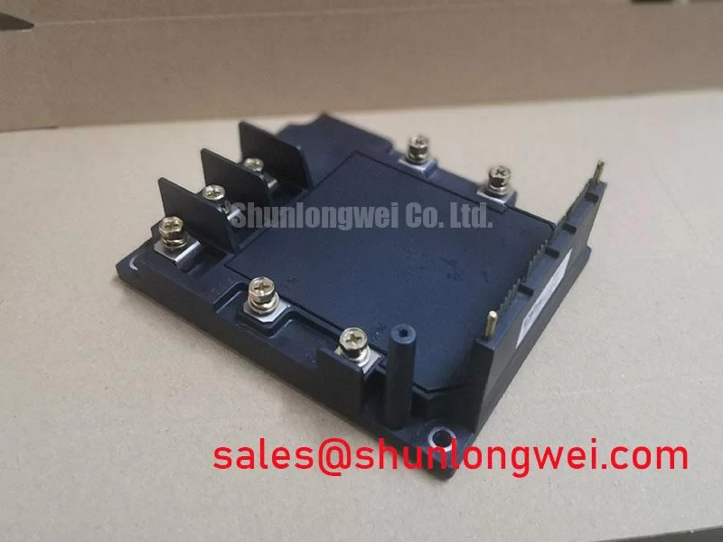
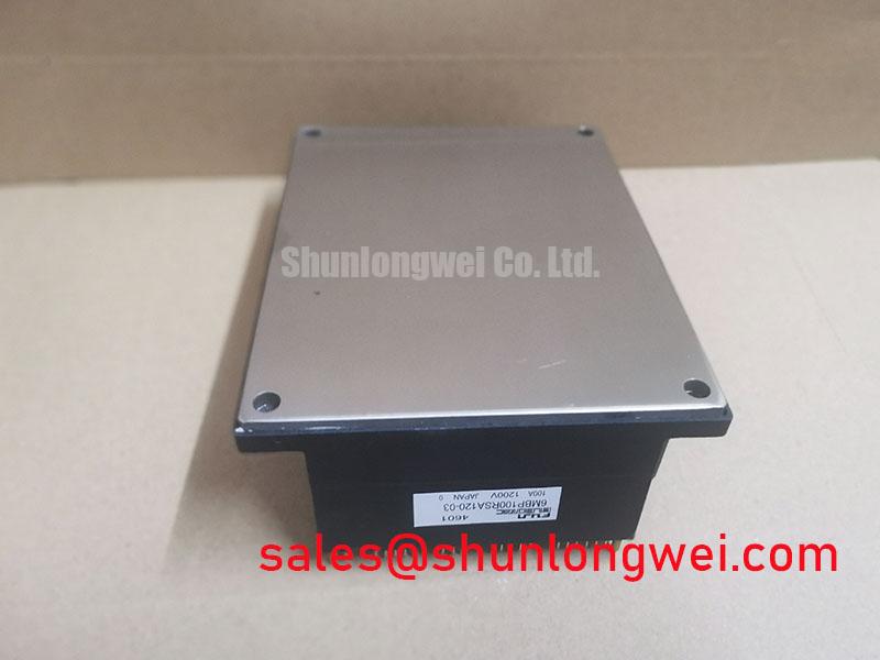
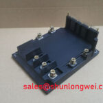
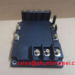
The 6MBP100RSA120-03 is a Fuji Electric IPM module with an official rated voltage of 1200.0 V and an official rated current of 100.0 A. Those values identify the module’s electrical class; they do not establish the allowable DC-link operating point, braking pulse duration, resistor energy rating, or thermal duty for a particular inverter welder or medium-frequency induction heating supply. The system designer must verify those conditions against the original circuit documentation and the applicable Fuji Electric data.
For a braking circuit, first record the DC-link voltage immediately before the fault and during the braking event. Check the voltage probe connection, probe bandwidth, and measurement reference because a long probe ground lead can create an apparent overshoot that is not representative of the module terminals. Compare the waveform at the power module with the waveform at the braking resistor terminals. A difference between these locations may indicate busbar inductance, loose mechanical joints, an unsuitable measurement loop, or an interrupted braking path.
The braking resistor must be assessed for pulse energy, repetition rate, cooling conditions, and failure behavior. Its continuous wattage alone does not establish suitability for repeated motor deceleration or energy recovery from an induction heating system. An engineering calculation should derive the resistor energy requirement from the actual DC-link voltage, load energy, braking interval, and duty cycle. The chopper transistor selection should then be checked against the resulting current pulse, switching loss, voltage overshoot, and junction temperature. These are system calculations, not additional factory ratings for this module.
Keep the high-current braking loop physically compact, with the positive and return paths arranged to reduce enclosed loop area. This is a Design Consideration intended to reduce parasitic inductance and turn-off overshoot. The final layout must be validated with a properly rated differential probe while the equipment operates at its intended current and switching conditions. Designers should verify that the measured peak voltage remains within the documented power-stage limits under the worst relevant operating condition.
When a braking fault appears only after the machine reaches operating temperature, inspect the resistor connections, cooling path, thermal switch, and driver supply under load. A resistor that measures correctly when cold can still develop an intermittent connection or excessive temperature rise during repeated braking. The module’s protection state should be checked through the control interface, while the gate-emitter signal should be compared with a known-good channel rather than judged from a single multimeter reading.
In an inverter welder, the front-end rectifier and the switching stage should be evaluated as one DC-link system. A separate power-module reference for topology review is the 7MBI100U4E-120. It is a separate product and should not be treated as an automatic substitute for any installed circuit. The complete chain includes rectification, DC-link capacitors, braking control, switching devices, current sensing, and the load network.
6MBP100RSA120-03 Thermal-Electrical Optimization: Baseplate Contact and Mounting Screw Practices
Check the contact pattern between the module baseplate and heatsink by inspecting the interface after controlled removal, then measure the heatsink flatness and look for dried or displaced thermal interface material. Uneven contact, excessive compound, or contamination can produce localized temperature rise even when the electrical waveform appears normal.
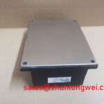
The Fuji Power Module package requires a mechanically stable thermal path selected for the actual dissipation and cooling arrangement. Thermal interface material should form a continuous, thin layer that fills surface irregularities without creating a thick insulating film. The commonly used 50 to 100 micrometre application range is a general Design Consideration, not a confirmed factory requirement for this specific model. The thermal-material supplier and the original assembly documentation should determine the accepted process window.
Baseplate curvature must be considered during heatsink preparation. A module should not be forced flat by excessive screw loading, because localized mechanical stress can affect the substrate, ceramic insulation, or terminal alignment. Clean both mating surfaces, remove old compound completely, and confirm that the heatsink does not rock when placed on a verified flat reference. If the original assembly uses a defined sequence, reproduce that sequence and use a calibrated torque tool.
Mounting torque is an assembly-process value rather than an electrical rating. The equipment builder should use the torque, screw type, washer arrangement, and tightening sequence specified for the original Fuji Electric package. A general M5 mounting range such as 2.5 to 3.5 N·m may be encountered in industrial assembly practice, but it must not replace the manufacturer’s instruction for this module and heatsink combination.
Maintenance Note: Monitor contact temperature during scheduled service and recheck the cooling fan path, heatsink cleanliness, and thermal interface condition before a rising thermal alarm becomes a switching fault.
The gate-drive supply also requires thermal and electrical review. For a high-side arrangement, bootstrap capacitor selection should account for gate charge, driver quiescent current, leakage, switching frequency, refresh interval, and the voltage tolerance of the driver supply. The capacitor value must be calculated from the complete driver charge budget and then verified during high-duty-cycle operation. A nominal capacitor value copied from another inverter is not sufficient evidence of gate-power integrity.
Inspect gate wiring separately from power wiring. Gate and emitter return conductors should follow a controlled path with minimal shared impedance, while the high-current collector and emitter loop should remain physically separated from sensitive control traces. Designers should verify the actual gate voltage at the module terminals, not only at the driver output, because connector resistance and common-emitter inductance can alter the signal during fast switching.
6MBP100RSA120-03 Operational Boundaries: Evaluating Thermal Feedback Limits
Compare the phase currents, collector-emitter voltage, gate-emitter waveform, and heatsink temperature at the same operating point when parallel current paths show unequal loading. This comparison helps distinguish gate-loop imbalance, busbar asymmetry, current-sensor error, and thermal differences without assigning a single cause prematurely.
The rated 100.0 A current is an official product parameter, but the usable current in an installed system depends on switching frequency, conduction duration, cooling performance, case temperature, gate-drive conditions, transient loading, and the limits defined by the applicable data sheet. A repair assessment should therefore compare measured electrical and thermal conditions with the original design envelope rather than treating the nameplate current as a universal continuous operating guarantee.
For devices operating in parallel, the positive temperature coefficient commonly associated with the on-state voltage can support static current sharing under suitable conditions. Dynamic sharing is more sensitive to gate-loop impedance, emitter-path inductance, propagation delay, busbar geometry, and driver behavior. Equal physical routing, equivalent terminal contact, and matched control timing are Design Considerations that require oscilloscope verification during the actual switching event.
When a module runs hotter than its corresponding channel, measure the voltage directly across the relevant power terminals under load and inspect the complete thermal interface. Also check whether one phase has a different cable length, laminated-busbar path, current-sensor position, or cooling exposure. Thermal feedback should be reviewed through the control system’s actual sensor placement and response time. A controller temperature value can lag the semiconductor junction behavior and should not be used as the only evidence of safe operation.
Bidirectional DC to DC battery charging and discharging systems deserve additional attention because repeated power reversal creates thermal cycling in the module, busbars, terminals, and heatsink assembly. Designers should evaluate the real current profile, dwell time, ambient conditions, cooling response, and switching transitions. Any lifetime projection requires an authoritative reliability model, mission-profile data, and validated thermal-cycle assumptions; unsupported operating-hour or failure-rate claims should not be used for this component.
Terminal inspection should include discoloration, looseness, oxidation, cracked insulation, and signs of uneven pressure. Measure contact resistance only with a method suitable for low-resistance power joints, and compare the result with a known-good connection under the same mechanical condition. High-voltage clearance and creepage must be preserved around the power terminals, contamination paths must be controlled, and condensation prevention should be considered for equipment exposed to low temperature, humidity changes, or unheated shutdown periods.
For topology selection in induction heating equipment, the system engineer may consult the neutral technical discussion on Resonant Topologies in Home Appliances. The article provides topology context, while the suitability of this Fuji Electric module remains dependent on the actual voltage, current, switching, cooling, insulation, and control requirements.
6MBP100RSA120-03 Circuit Protection & Reliability: Suppressing Parasitic-Capacitance-Induced Gate Voltage Spikes
Capture the off-state gate-emitter voltage on the inactive switch while the opposite device turns on, using a short differential measurement loop at the module terminals. A transient gate rise during high dv/dt operation may indicate capacitive coupling, common-emitter inductance, driver impedance, or an unsuitable return path; verify the signal against the known-good switching channel before changing the protection circuit.
The relevant parasitic capacitance can inject displacement current into the gate circuit during a rapid collector-voltage transition. The resulting disturbance is influenced by the power-module layout, gate resistor, driver output impedance, emitter reference, isolation arrangement, and switching conditions. A dedicated Miller clamp can provide a low-impedance off-state path when correctly coordinated with the driver timing. Its effectiveness must be established by measuring the gate voltage at the module pins during turn-on and turn-off transitions.
Negative gate bias may be considered where the driver and module documentation explicitly support it. The often-discussed range of minus 5 V to minus 15 V is a general engineering reference, not a confirmed rating for the 6MBP100RSA120-03. The actual gate-emitter voltage limits, driver supply arrangement, isolation requirements, and turn-on threshold must be taken from the applicable Fuji Electric documentation. Designers should verify that the negative bias does not exceed the allowed gate-emitter stress or create unwanted behavior during power sequencing.
Soft shutdown and desaturation protection should be evaluated together. A desaturation event may result from a short circuit, insufficient gate drive, excessive commutation voltage, sensor timing, or a fault in the load path. The protection circuit should detect the abnormal condition, control the turn-off transition, record the fault state, and prevent immediate re-energization until the DC link and gate-drive supplies have been assessed. Short-circuit safe operating behavior must be confirmed from the manufacturer’s specified test conditions rather than inferred from the 1200.0 V voltage class.
Keep the gate-driver loop separate from the collector switching loop and route the driver return to the intended emitter reference. Avoid sharing a narrow control trace with high-current commutation paths. Verify the driver’s undervoltage lockout, isolation supply stability, dead time, fault reset behavior, and connector retention. A gate waveform that is correct at the driver board but distorted at the module terminal points to an interconnect or layout problem that should be resolved before another power module is installed.
Fuji Electric’s Power Semiconductor and IPM Modules information and its Power Semiconductors Portal provide the appropriate manufacturer-level context for confirming device family information and application documentation. This product page identifies the supplied hardware class and official headline ratings; final gate protection, insulation coordination, thermal limits, and switching validation remain functions of the complete equipment design.