

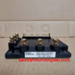
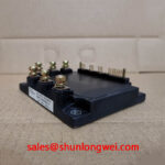
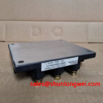
Content last revised on November 4, 2026
Preventing Spurious Faults: Auxiliary Emitter Return Trace Separation Guidelines for 7MBP150RA060-01
Separate the auxiliary emitter return from the main high-current emitter trace wherever the circuit layout permits. The reason is common impedance coupling: the voltage developed across a shared return path during switching can appear at the gate-drive reference and disturb the intended gate-to-emitter command. This can present as irregular turn-on, unexpected turn-off behavior, gate-driver protection activity, or waveform ringing that changes with load current.
This is a Design Consideration, not an additional Fuji Electric rating. The module’s official identity remains 600.0 V, 150.0 A; the stability of the complete switching loop depends on the gate driver, PCB geometry, busbar arrangement, current commutation path, and control-board isolation strategy. When integrating the module, designers should keep the gate-drive loop compact, avoid routing the auxiliary return beside noisy switching nodes, and verify the reference potential directly at the module terminals during switching tests.
For a field repair, begin by photographing the original conductor positions and identifying whether the control board uses an auxiliary emitter connection or a shared emitter reference. Inspect crimped lugs, plug contacts, solder joints, and board-to-module wiring for looseness or discoloration. A damaged return connection can create symptoms that resemble a failed power semiconductor, especially when the equipment trips only during higher-current operation.
Oscilloscope verification should compare the gate-to-emitter signal at the module with the corresponding signal at the driver output. A difference between these points may indicate return-path inductance, common-emitter coupling, probe-ground interference, or a control-board fault. Use an appropriate differential measurement method and keep the probe connection physically short. The test objective is to confirm that the gate signal remains within the driver’s intended operating behavior while the power loop is switching.
Designers evaluating an industrial inverter welder or medium-frequency induction heating power stage should also review the isolation barrier and common-mode transient response of the driver. A digital isolator or optocoupler must be assessed as part of the control system, including its common-mode transient immunity, propagation delay, supply decoupling, and fault-state behavior. These characteristics are system-level compatibility factors and are not stated here as individual specifications of the 7MBP150RA060-01.
Gate resistance, Miller plateau behavior, and active clamp operation should be tuned from measured switching waveforms rather than copied from an unrelated module. The relevant checks include gate overshoot, false gate movement during the opposite device’s transition, collector-emitter overshoot, and the driver’s response to a desaturation or overcurrent event. The engineering aim is to control parasitic coupling while maintaining the switching speed required by the equipment topology.
For background on gate-loop behavior and switching-control layout, engineers can consult the Precision Gate Drive Design guide. The Fuji Electric Power Semiconductor and IPM Modules resource is also relevant when reviewing the manufacturer’s broader module product context.
Field Alert: Isolate DC-link power and confirm the discharge state before disconnecting gate-drive or auxiliary-emitter wiring.
7MBP150RA060-01 Assembly and Protection Considerations
Mechanical flatness must be checked before applying thermal interface material. A convex copper baseplate, a damaged heatsink surface, or uneven fastener loading can concentrate mechanical stress through the ceramic substrate and reduce thermal contact. Place a straightedge across the heatsink mounting area, remove old compound completely, and inspect for raised burrs, embedded particles, or localized corrosion. These checks are general assembly practice and are not additional official ratings for this model.
The thermal interface layer should be continuous and uniform rather than thick enough to mask a poor heatsink surface. Use a layer appropriate to the selected thermal compound, surface finish, and mounting system. The system engineer should verify the resulting thermal resistance and mechanical stress under the actual installation conditions.
Fasteners should be tightened progressively in a diagonal cross-pattern so that the baseplate seats evenly. The required torque is determined by the fastener size, thread condition, washer arrangement, heatsink material, and the module manufacturer’s mechanical documentation. Do not treat a generic torque value as an official specification for this part. After tightening, recheck that the module has not shifted and that the thermal compound has spread across the intended contact area.
The electrical protection sequence needs the same discipline. A desaturation circuit can detect an abnormal collector-emitter condition and initiate a controlled shutdown, but the detection threshold, blanking interval, sensing method, and driver output behavior are properties of the complete gate-drive design. The required response time should be determined from the equipment topology and validated as part of the protection design; it is not an official timing specification of the 7MBP150RA060-01.
Two-stage soft turn-off is a Design Consideration for limiting the voltage excursion caused by abruptly interrupting fault current. The first response can reduce gate drive in a controlled manner, while the final state disables the device and reports the fault to the controller. The correct sequence depends on short-circuit current, stray inductance, gate-driver capability, protection delay, and the DC-link arrangement. Validate the complete sequence with the actual protection circuit and switching waveform.
| Parameter | 7MBP150RA060-01 | 7MBR15SA060D-01 |
|---|---|---|
| Manufacturer | Fuji Electric | Fuji Electric |
| Official listed voltage rating | 600.0 V | Consult product documentation |
| Official listed current rating | 150.0 A | Consult product documentation |
| Package classification | Fuji Power Module | Consult product documentation |
The comparison above is a sourcing aid, not a declaration of pin-for-pin interchangeability. Engineers assessing a related Fuji Electric device can review 7MBR15SA060D-01, then compare terminal markings, internal topology, gate-drive requirements, protection behavior, mechanical dimensions, and thermal interface details against the original equipment documentation. A similar voltage or current label alone does not establish a valid replacement.
Overvoltage coordination should include the complete commutation loop. An MOV, snubber, clamp, or active gate-control network may be used depending on the DC-link structure and switching energy, but its voltage rating, energy capability, placement, and coordination with the module must be selected by the system designer. The purpose is to keep transient stress within the verified switching and insulation margins of the equipment, with the final values confirmed during controlled testing.
7MBP150RA060-01 Cold-State Checks and Reliability
Perform the first electrical screen with the equipment unpowered and the DC link discharged. Use the digital multimeter’s diode-check function across the main terminals in both polarities, then compare the results with the expected circuit topology and the known-good phase leg. The antiparallel diode path should be evaluated in the direction shown by the original schematic. Avoid interpreting a single meter display as a complete semiconductor health verdict because connected capacitors, snubbers, resistors, and gate-drive components can influence the reading.
Before measuring, disconnect the module from the control board and isolate parallel power paths where the equipment design allows. Record polarity, test lead direction, meter mode, and whether the reading stabilizes or changes over time. A persistent short indication, an open path where the circuit should conduct, or a marked difference between equivalent phase legs warrants further isolation testing. These observations guide the next measurement; they do not by themselves identify the precise failure mechanism.
Gate leakage screening should be performed with the gate terminals isolated from the driver and with the meter’s test voltage kept within the limits appropriate to the gate structure. Compare gate-to-emitter behavior in both polarities and compare equivalent channels when the module topology provides them. Unstable readings can result from contamination, residual charge, measurement contact problems, or damage to the gate-control circuit. Clean, dry connections and repeatable probe placement are essential for a useful comparison.
After the cold-state screen, inspect the main terminals for heat discoloration, loosened hardware, surface oxidation, or evidence of arcing. Check the conductor lugs and busbar contact faces as well as the module terminals. A sound semiconductor can still fail in service when a high-current joint has excessive contact resistance or when the busbar applies mechanical force to the package. Confirm that the replacement module sits without forced alignment before reconnecting the conductors.
For an industrial inverter welder, verify the current sensor path, driver enable signal, fault-reset sequence, and cooling interlock before applying full operating power. For a medium-frequency induction heating supply, also review the resonant network, commutation timing, and overvoltage clamp behavior because the module sees the combined effect of the switching bridge and its load network. These applications are compatibility examples; the equipment manufacturer’s circuit documentation determines the required control and protection conditions.
Positive temperature coefficient behavior can support current sharing between paralleled devices, but it does not remove the need to match layout resistance, gate-drive timing, emitter-return geometry, thermal coupling, and dynamic switching behavior. Static sharing should be checked at the intended operating point, while dynamic sharing requires waveform measurement during turn-on and turn-off. Any parallel arrangement must be validated as a complete power stage rather than inferred from the current rating printed on one module.
Before energization, confirm the module rating identity, terminal polarity, gate-drive reference, insulation clearances, heatsink contact, protection interlocks, and fault logging path. Apply power through the equipment’s controlled commissioning procedure and observe the first switching events with suitable voltage and current probes. Check for abnormal gate movement, unexpected phase imbalance, excessive switching-node ringing, and protection activation before moving toward normal load operation.
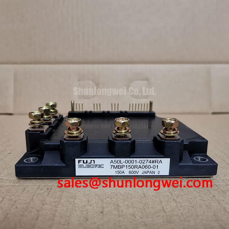
The 7MBP150RA060-01 remains identified by its official 600.0 V voltage rating, 150.0 A current rating, and Fuji Power Module package classification. Those values establish the product reference; successful field integration depends on matching the original terminal arrangement, thermal assembly, gate-drive return path, protection timing, and equipment-level switching conditions.