




Content last revised on September 29, 2026
2MBI600VE-120 Circuit Protection & Reliability: Calibrating DC-DC Converter Interleaving and Ripple Current
| Manufacturer | Fuji Electric |
| Model | 2MBI600VE-120 |
| Product category | IGBT Module |
| Rated voltage | 1200.0 V |
| Rated current | 600.0 A |
| Package | Fuji Power Module |
Probe the DC link, phase output, and gate command with suitably rated differential or isolated voltage probes when a battery energy storage PCS shows ripple growth, uneven phase loading, or repeated converter trips. Compare the current waveform of each interleaved leg at the same operating point, then inspect whether the disturbance follows the power path, gate-drive path, or measurement circuit.
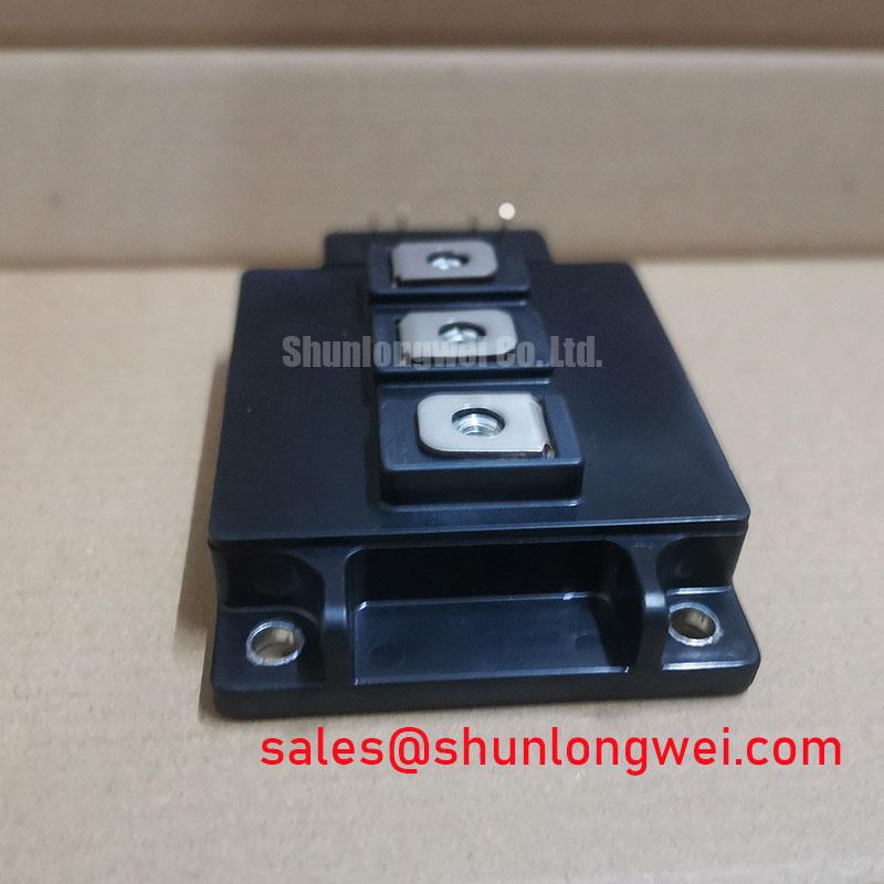
The 2MBI600VE-120 is a Fuji Electric IGBT module with an official rated voltage of 1200.0 V and an official rated current of 600.0 A. Its package is identified as a Fuji Power Module. These are component ratings, not permission to operate a complete PCS at the same limits. The system designer must verify switching frequency, duty cycle, pulse current, thermal conditions, commutation behavior, and the applicable device derating method from the original Fuji Electric documentation.
In a centralized battery storage PCS, power can move from the battery racks toward the inverter link during discharge and reverse direction during charging or grid-support operation. The bidirectional operating sequence changes the current direction and the active switching devices, so a ripple problem should be checked in both power-flow directions. Record the DC-link voltage, phase current, gate-emitter waveform, and heat-sink temperature during controlled tests rather than judging the module from a single current reading.
Interleaved DC-DC stages require matched timing and comparable impedance in each commutation loop. A small difference in gate resistance, driver propagation delay, busbar path, or current-sensor placement can redistribute dynamic current between legs. This is a Design Consideration rather than a guaranteed behavior of the module. Keep the high-current paths physically symmetrical where the system topology allows it, and validate the result with simultaneous current probes.
Ripple current also interacts with the freewheeling path. The reverse-recovery softness factor of the associated diode network can influence switching overshoot, common-mode current, and radiated EMI. The diode characteristics of the complete commutation path must be confirmed from the relevant circuit documentation; they should not be inferred from the 2MBI600VE-120 name alone. Fuji Electric’s IGBT module application information provides useful manufacturer context for chopper-related power semiconductor evaluation.
For regenerative braking or DC-link energy absorption, inspect the chopper branch, braking resistor, snubber network, and control interlock as one circuit. A high-energy braking event can expose stray inductance and protection timing that remain invisible during low-power testing. The resistor’s thermal duty, pulse capability, and enclosure cooling are system-level matters. Do not treat the module’s voltage and current ratings as a substitute for a complete transient and energy calculation.
When a related topology is being reviewed, engineers may also compare the neutral information available for 2MBI25L-120. That link is a separate product reference, not an automatic substitute. Voltage, current, electrical configuration, mechanical fit, gate-drive behavior, and thermal performance must all be checked before any cross-model evaluation.
Assembly Integrity & Layout Architecture: Implementing Thermal Feedback for 2MBI600VE-120
Measure the temperature rise at the module baseplate, the heat-sink inlet and outlet, and each parallel current path when static current sharing appears uneven. Then compare the gate-emitter voltage and collector-emitter waveform of each device under the same load, because a thermal imbalance and a dynamic drive mismatch can produce similar symptoms.
Parallel IGBT modules require a busbar arrangement that presents comparable electrical impedance to every branch. Keep collector and emitter paths symmetrical, avoid routing one branch around a larger mechanical obstruction, and place current measurement points so that they do not unintentionally add different loop inductances. The gate-drive wiring should follow the same principle. Separate power-current conductors from gate-control conductors and route corresponding gate loops with closely matched length and coupling.
The positive temperature coefficient commonly associated with IGBT saturation voltage can support static current sharing in parallel operation: as a device warms, its voltage behavior can oppose further current concentration under suitable operating conditions. This is a Design Consideration, not a complete guarantee of balanced dynamic current. During switching, parasitic inductance, driver delay, gate resistance, diode recovery, and busbar geometry may dominate the sharing behavior.
Use thermal feedback as a diagnostic signal rather than as the sole protection input. A temperature sensor on the heat sink may respond more slowly than the semiconductor junction, while a current probe can reveal short-duration imbalance that never appears in the average thermal reading. When the PCS controller changes between charge and discharge, capture both transitions and compare the module branches at equivalent power levels.
Mounting surfaces should be clean, flat, and free from old, hardened thermal material. Apply the selected interface material consistently according to its manufacturer’s process guidance, and confirm that the fastening method produces even contact across the baseplate. Maintenance Note: monitor contact temperature rise during scheduled service and check that dust accumulation has not restricted the heat-sink airflow.
High humidity and condensation deserve attention in storage conversion rooms that cycle between warm and cool conditions. Inspect for moisture around insulated busbars, gate-driver connectors, and heat-sink interfaces before energization. The environmental suitability of the complete assembly depends on the enclosure, heater or dehumidification strategy, insulation system, and site conditions; no independent EMC, insulation, or environmental certification should be inferred from the module specification alone.
For a system containing a front-end rectifier or complementary conversion stage, the 6MBI180VX-120-55 can be reviewed as a separate related device reference. It should not be treated as a prescribed pairing with the 2MBI600VE-120. Confirm topology, control timing, current path, cooling arrangement, and the original equipment documentation before integrating any related part.
2MBI600VE-120 Operational Boundaries: Evaluating Transient Thermal Impedance Limits
Capture the load pulse, collector-emitter voltage, and case or heat-sink temperature together when a PCS experiences overload trips after a short peak-shaving interval. The time relationship between the electrical pulse and measured temperature helps distinguish a thermal accumulation problem from a switching overshoot or protection-threshold event.
The official data supplied for this product identifies a 1200.0 V voltage rating and a 600.0 A current rating. Those values define important component boundaries, but they do not by themselves define allowable overload duration, transient thermal impedance, junction temperature, short-circuit withstand, or safe operating area. Such limits must be taken from the applicable Fuji Electric data sheet and evaluated against the actual mounting, switching, cooling, and pulse conditions.
For a pulsed overload, an engineering calculation may represent the junction-to-case response with a manufacturer-provided multi-RC thermal model. The resulting junction-temperature estimate depends on the initial case temperature, pulse duration, duty cycle, heat-sink impedance, interface condition, and the correct transient thermal data. If the original model is unavailable, do not create a substitute RC network from nominal package ratings; use controlled thermal testing and obtain the required device data before approving the operating envelope.
Heavy C-rate peak shaving can create cyclic thermal swings even when the average converter power appears acceptable. Review the highest and lowest thermal points over repeated charge and discharge cycles, then inspect the heat-sink fan curve, filter loading, duct leakage, and cabinet recirculation. A clean heat sink does not compensate for a blocked inlet or a fan operating outside its intended control range.
Minimize the commutation loop area and verify physical clearance around high-voltage conductors to reduce the likelihood of inductive overshoot and unwanted coupling. The appropriate clearance and insulation coordination are determined by the DC-link voltage, pollution environment, altitude, enclosure construction, and applicable safety design rules. Validate peak voltage at the module terminals during switching tests, not only at a remote DC-link sensor.
A thermal imbalance between parallel modules should be investigated through several measurements: branch current, gate timing, collector-emitter voltage, baseplate temperature, and interface condition. A single hot spot does not prove one specific failure mechanism. Compare the affected branch with a known-good operating phase and repeat the measurement after checking the driver supply, current transducer, cooling path, and mechanical contact.
Practical integration references for gate-drive layout, thermal management, and power-conversion topology are available in IGBT Design & Integration. Use such guidance as an engineering reference while retaining the original Fuji Electric limits as the controlling source for device-specific decisions.
Benchtop Waveform Tuning: Mitigating Hard Switching Transients on 2MBI600VE-120
Connect differential voltage probes and isolated current probes at the module terminals before changing the gate-drive resistor when a bench waveform shows excessive turn-off overshoot or ringing. Verify probe bandwidth, grounding method, and probe loop area first, because an unsuitable measurement setup can create an apparent transient that is not present in the power circuit.
Hard-switching stress is affected by stray inductance, gate-loop impedance, driver source and sink capability, diode reverse recovery, DC-link capacitor placement, and the load current at the switching instant. The relationship between inductance and current slew rate means that reducing the commutation loop and controlling the turn-off transition can reduce peak overshoot, but the final gate-drive setting must be established through measured voltage, current, switching loss, and thermal results.
Keep the gate command path separate from the high-current emitter path, and follow the module’s actual terminal arrangement rather than assuming a Kelvin emitter or auxiliary emitter connection that is not confirmed by the applicable terminal drawing. A separate low-inductance gate return can improve measurement consistency where the package provides the required connection, but the system integrator must verify the terminal definition and recommended drive circuit for this exact module.
Short-circuit protection should be evaluated with the controller, driver, sensing method, and module as one protection chain. Type I and Type II short-circuit behavior, short-circuit safe operating area, and any sub-ten-microsecond detection claim require direct support from the applicable manufacturer documentation and test conditions. They cannot be assigned to the 2MBI600VE-120 from the model number alone.
A two-stage soft turn-off sequence is a possible Engineering Recommendation for reducing the rate of current interruption during a detected fault. The first stage can limit the immediate transition, while the second stage completes turn-off under the driver’s verified voltage and current conditions. The actual timing, gate voltage, resistance, desaturation method, and fault blanking must be determined by the system designer and validated with the module’s short-circuit limits.
When tuning a regenerative chopper or inverter leg, check the turn-on and turn-off waveforms in both current directions. A waveform that appears stable during motoring operation may show different recovery behavior during regenerative braking because the active switch, freewheeling path, and current commutation sequence have changed. Evaluate the associated braking resistor and snubber energy as part of the same test plan.
Record the DC-link voltage, peak collector-emitter voltage, gate-emitter voltage, current slew, switching loss, and case temperature for each test condition. Stop the test when measured margins approach the applicable device or system limit, and allow the thermal state to return to the defined starting condition before comparing another waveform. This produces a defensible engineering record without treating an unverified bench result as a guaranteed field operating limit.