Content last revised on September 10, 2026
6MBP30RY060 Operational Boundaries: Evaluating PCB Symmetry Considerations for Dual IGBT Limits
Before installation, isolate the drive, discharge the DC link, and compare cold-state terminal readings with a known-good assembly or the original service record; unexpected low resistance between power terminals can indicate a damaged external circuit or a failed module and requires controlled investigation.
The Fuji Electric 6MBP30RY060 is a 600 V, 30 A six-pack IGBT module with free-wheel diodes arranged as a three-phase bridge. Its official ratings provide a defined electrical boundary for repair assessment and inverter integration in precision stepper and BLDC motor servo motion actuators. The module is rated at VCES = 600 V, IC = 30 A at TC = 25°C, and a maximum junction temperature of 150°C.
| Official Specification | Value | Condition |
|---|---|---|
| Collector-emitter voltage | 600 V | VCES |
| Collector current | 30 A | TC = 25°C |
| Collector-emitter saturation voltage | 2.7 V maximum | IC = 30 A, Tj = 25°C |
| Free-wheel diode forward voltage | 3.5 V maximum | −IC = 30 A, Tj = 25°C |
| Total power dissipation | 85 W | One transistor, TC = 25°C |
| Junction temperature | 150°C | Maximum rating |
| Configuration | 6-pack IGBT plus FWD | Three-phase bridge |
Each switching leg in a three-phase bridge has to be evaluated as part of a complete commutation loop, not as an isolated transistor. For the 6MBP30RY060, the 600 V blocking rating and 30 A collector-current rating are Official Datasheet Specifications, while the achievable operating margin depends on the DC-link condition, load inductance, gate-drive behavior, cooling arrangement, and measured switching waveform.
A Design Consideration is to keep the high-current collector and emitter loop physically compact and geometrically balanced across the three phases. Gate-drive return conductors should not share an extended high-current emitter path, because the voltage developed across shared parasitic inductance can alter the effective gate-emitter voltage during switching. This coupling may present as unequal ringing, phase-specific gate disturbance, or inconsistent switching waveforms even where the DC resistance of the power paths appears similar.
When the module terminal arrangement and driver architecture permit it, route the gate-drive reference independently from the main high-current return path. The system integrator should verify the actual terminal functions from the original module documentation and drive-board schematic rather than assuming that a separate auxiliary emitter connection is available. Keep each phase gate loop comparable in length, routing environment, and return path so that observed differences are easier to trace during commissioning.
For a servo actuator repair, inspect busbar contact faces, mounting-plane flatness, gate connector seating, and phase output routing before applying power. Then use an isolated low-voltage driver check and oscilloscope measurement against a known-good signal path. Ringing or unexplained gate movement may indicate common-emitter coupling, unsuitable probe grounding, driver-reference disturbance, or an external layout issue. ⚡ Safety Interlock Note: Never connect or remove gate-drive or power wiring until the DC link is verified discharged and locked out.
💡 Pro Tip: Use symmetrical DC-link busbar geometry around the bridge to reduce turn-off loop inductance, then verify peak voltage and gate stability with double-pulse testing under the actual system conditions.
6MBP30RY060 Operational Boundaries: Evaluating High dv/dt Cross-Conduction Shoot-Through Limits
High dv/dt at a switching node can transfer displacement current through the reverse-transfer capacitance of an off-state IGBT. If that current raises the off-state gate voltage sufficiently, temporary cross-conduction can occur within an inverter leg. This is a system-level behavior, not an official claim about the 6MBP30RY060 alone, and it should be investigated by measuring gate-emitter voltage at the module-side drive reference during representative switching events.
A dedicated low-impedance active Miller clamp is a Design Consideration where the driver supports that function. Negative gate bias is also commonly evaluated in industrial IGBT drive circuits, often within a −5 V to −15 V range as a general industry design range, not as an official operating prescription for this module. The required gate-drive levels, clamp threshold, dead time, gate resistance, and protection timing must be determined by the complete driver, load, and switching test results.
The mounting interface matters because temperature variation changes conduction loss and switching behavior. The official maximum VCE(sat) of 2.7 V at 30 A and 25°C is useful for loss assessment, but it is not a substitute for thermal validation at the intended case temperature and switching duty. A 50 to 80 μm thermal interface material bond line is a General Industry Design Consideration when the heatsink flatness, material guidance, and mounting method support it. Apply the specified mounting torque in a cross-pattern sequence according to the applicable mechanical documentation.
During troubleshooting, compare all three phase gate waveforms and switching-node transitions using measurement methods that preserve bandwidth and minimize probe-loop pickup. A waveform that appears to show shoot-through can also be distorted by measurement setup. Confirm the result with a differential method and correlate it with DC-link current, driver supply stability, and protection-event records.
For broader device-family context, consult the Fuji Electric Power Semiconductors Portal when reviewing power-module technology and manufacturer resources.
6MBP30RY060 Circuit Protection & Reliability: Calibrating Multi-Module Parallel Current Sharing
Paralleling bridge modules should be treated as a dedicated system design task. The 6MBP30RY060 is specified as one six-pack IGBT plus FWD three-phase bridge; its published ratings do not establish a guaranteed current-sharing result with additional modules. In steady operation, IGBT conduction behavior can support thermal current balancing over an appropriate operating region because VCE(sat) often has a positive temperature coefficient. Dynamic sharing, however, is strongly influenced by busbar symmetry, gate-loop impedance, driver timing, and current-sense placement.
An Engineering Recommendation is to make parallel power paths electrically and physically comparable, including DC-link connections, AC phase links, gate routing, and cooling conditions. Verify sharing through measured phase current and switching waveforms at the real load rather than inferring balance from equal conductor lengths alone. Current imbalance may be caused by tolerances, unequal thermal paths, driver timing deviation, or layout coupling, so each condition should be checked independently.
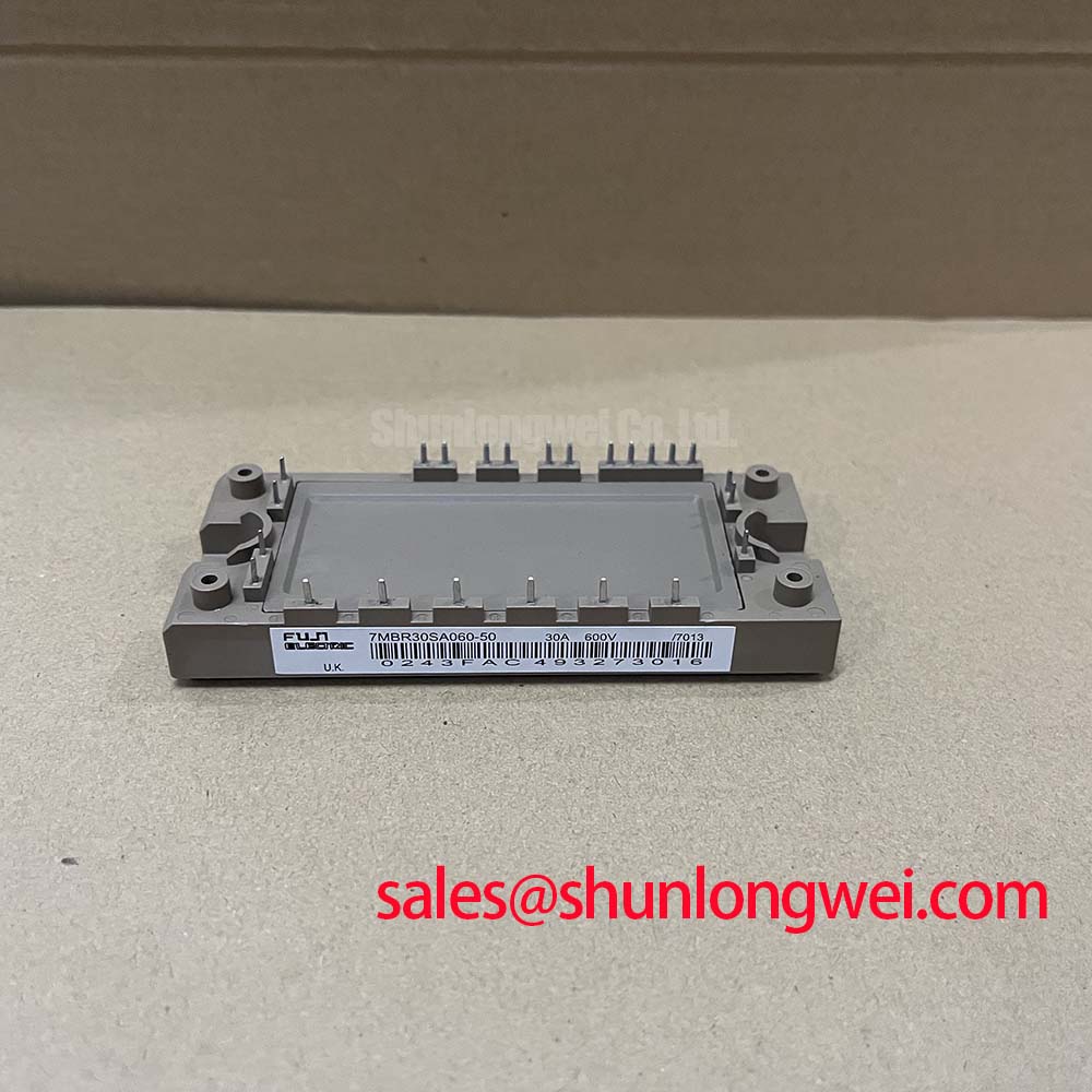
For systems that include a separate front-end conversion stage, the 7MBR50SB120-01 can be reviewed as a related module for topology-level evaluation. Its electrical and mechanical details must be compared independently; it should not be treated as an automatic counterpart or replacement.
Where a service team is assessing another bridge-module option, the 7MBR50LC060 is available for objective comparison of published voltage rating, current capability, pin arrangement, driver requirements, mechanical interface, and thermal implementation. A direct replacement decision requires verification of every relevant system interface.
6MBP30RY060 Thermal-Electrical Optimization: Fault-Clearing Dynamics: Type-I/II Desatur Practical Tuning
Desaturation protection should be coordinated with the actual inverter fault behavior rather than tuned only from nominal current. Under a short-circuit or severe overcurrent event, collector-emitter voltage rises while gate drive remains active. A desaturation circuit monitors that condition and commands turn-off before the device exceeds the applicable short-circuit safe-operating boundary. The official information provided for this module specifies 150°C as the maximum junction temperature but does not provide a short-circuit duration rating; therefore, no specific withstand time should be assumed.
Type-I and Type-II desaturation approaches can differ in their blanking, threshold processing, and response architecture. For fault-clearing targets below 10 μs, a General Industry Protection Consideration is to validate the entire chain: sensor path, comparator behavior, isolation delay, gate-driver response, and the module voltage waveform. The final response time must be verified against the module documentation, fault current rise, DC-link voltage, and measured test results.
Two-stage soft turn-off is often assessed where abrupt gate removal could create excessive inductive overvoltage. The underlying principle is to control the fault turn-off transition while ensuring that the remaining energy is managed by the complete protection system. DC-link layout, snubber arrangement, fuse coordination, and controller fault handling are system-determined. Semiconductor fuse selection should consider the actual fault-energy and I²t coordination data supplied by the fuse manufacturer and the inverter designer.
Thermal review should combine the case-to-heatsink interface with the duty cycle and transient thermal impedance information available from the relevant manufacturer documentation. Measure heatsink temperature, evaluate phase loading, and review fault logs after controlled testing. For application perspectives involving renewable energy, electric drives, and industrial conversion equipment, see Industrial Applications. Additional regional semiconductor and power-electronics resources are available from Fuji Electric Europe Semiconductor & Power Electronics.