

Content last revised on September 2, 2026
Kelvin Emitter Connection & Parasitic Inductance Minimization in High-Speed Switching
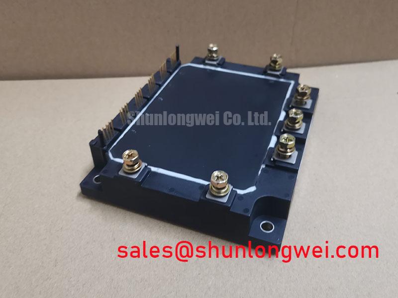
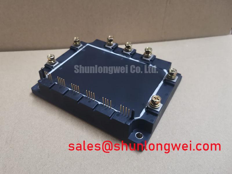
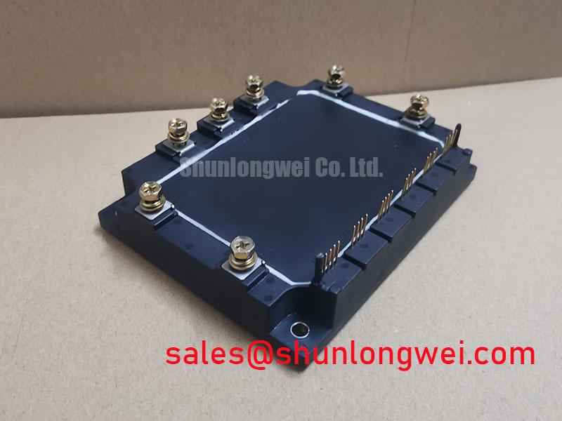
Static incoming inspection of the 6MBP300RA060 Intelligent Power Module (IPM) requires strict isolation between signal ground loops and high-current paths. Rated at 600.0V and 300.0A (Official Datasheet Specification), this 6-pack module integrates dedicated internal drive circuitry alongside Fuji Electric's IGBT silicon. When evaluating modules on the incoming bench, the auxiliary Kelvin emitter terminal must show complete galvanic separation from the power emitter plane until the internal monolithic junction. Mutual inductance between the high-current switched emitter and the control gate-emitter loop can introduce severe parasitic voltages during fast switching transients. If stray loop inductance is present, high di/dt will induce a reverse potential across the gate return path, causing unwanted negative feedback, gate signal distortion, or unintended cross-conduction.
💡 Bench Tip: Before applying control bias, set your digital multimeter to the diode test range to measure the cold-state forward drop of the integrated freewheeling diodes between each phase output and DC bus terminal. At 25°C ambient, expect a standard forward drop reading between 0.35V and 0.55V across the antiparallel diodes (Typical Starting Point for incoming screening). Always maintain ESD wrist straps grounded through a 1 MΩ resistor; static charges on the logic input pins (IN_U, IN_V, IN_W, and their lower-arm complements) can puncture internal CMOS buffer stages without exhibiting immediate catastrophic package rupture.
Minimizing external loop inductance requires a symmetrical laminated busbar design directly above the module terminals. Keep the AC phase copper and the DC positive/negative conductors tightly stacked, separated only by thin high-dielectric insulation sheets (such as 0.25 mm Nomex or Kapton). In commercial string inverter layouts, keeping the Kelvin drive tracks routed as tightly coupled differential pairs directly to the interface connector minimizes radiated EMI pickup. For engineers maintaining older system hardware or evaluating alternate single/dual-switch sub-assemblies, discrete topologies like the 1MBI300L-060 provide a baseline reference for direct single-switch phase branch configurations.
| Parameter | Official Datasheet Specification | Verification Condition / Method | Status / Classification |
|---|---|---|---|
| Collector-Emitter Voltage (VCES) | 600.0V | Tj = 25°C, Gate-Emitter shorted | Official Specification |
| Continuous Collector Current (IC) | 300.0A | Tc = 100°C continuous operation | Official Specification |
| Isolation Voltage (Viso) | 2500V AC (1 min) | 50/60 Hz applied between terminals & baseplate | Official Specification |
| Control Supply Voltage (VCC) | 13.5V to 16.5V (15.0V Typ.) | Applied across VCC and GND pins | Official Specification |
Dynamic Gate Impedance Control for Robust Phase-Leg Dead-Time Operation
Operating a 300A-class IPM in commercial string inverters and micro-grid energy storage racks demands strict control over dead-time settings and internal dv/dt dynamics. The integrated gate drive stage within the 6MBP300RA060 incorporates built-in drive resistors and active circuitry optimized by Fuji Electric Power Semiconductor & IPM Modules to control turn-on and turn-off slopes. However, high transient dv/dt generated during the opposite switch's transition can inject displacement currents into the gate through the collector-gate Miller capacitance (Cres). If this current encounters an elevated gate impedance, it lifts the internal gate voltage above the threshold level, risking phase-leg shoot-through.
When verifying peripheral driver interface boards, ensure the control logic provides a minimum dead-time of 2.0 to 2.5 µs (Design Consideration for 600V IPM architectures). The internal control IC provides built-in under-voltage lock-out (UVLO) and over-current protection with soft turn-off shutdown. Thermal derating must be strictly applied across the chosen pulse-width modulation (PWM) carrier frequency range:
- 2 kHz to 8 kHz Carrier Operation: Optimal for high-current micro-grid energy storage where conduction losses dominate; yields minimum thermal stress on internal gate driver ICs.
- 8 kHz to 16 kHz Carrier Operation: Produces lower acoustic noise and reduced AC filter inductor sizing, but requires forced-air convective cooling velocity exceeding 4.0 m/s across the heatsink fins to offset elevated switching losses.
⚠️ Field Alert: When retrofitting or repairing legacy motor drive or inverter stages, verify that the optocoupler isolators driving the IPM inputs have a minimum Common Mode Transient Immunity (CMTI) of at least 15 kV/µs. Using general-purpose optocouplers with low CMTI will cause false pulse triggering during high-speed switching transitions, leading to catastrophic phase-to-phase short circuits.
Thermal Feedback & V_CE(sat) Positive Temperature Coefficient Equalization
The collector-emitter saturation voltage VCE(sat) exhibits a positive temperature coefficient at higher current densities, an essential physical trait for parallel operational balance. When the silicon die temperature increases, the carrier mobility drops, causing VCE(sat) to rise slightly under heavy load. This naturally forces excessive current to redistribute across cooler regions of the die or adjacent parallel modules, preventing localized thermal runaway.
During incoming quality testing, measuring the static forward voltage across the collector-emitter path requires a precision pulsed high-current bench source. Supplying a short 300 µs pulse at 300.0A with a nominal 15V gate bias reveals the true static VCE(sat) without heating the internal junction. Values consistently reading within standard tolerance (typically 1.70V to 2.30V at 25°C) indicate normal silicon characteristics. For complementary subsystem architectures or discrete half-bridge designs requiring independent drive circuitry, engineers often compare these baseline parameters against dual-pack modules such as the 2MBI300J-060.
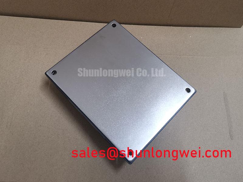
The module baseplate features an integrated, galvanically isolated thermistor that delivers continuous thermal feedback to the external control system. When mounting the module to a machined heatsink, apply a uniform layer of silicone-free or standard high-performance thermal grease with a target thickness of 60 to 100 µm (General Industry Design Consideration). Fasten the baseplate screws using a two-step torque sequence: initial pre-tightening to 1.0 N·m across all mounting holes, followed by final torque between 2.5 and 3.5 N·m in a diagonal criss-cross pattern. This prevents substrate warping and micro-cracking of the internal ceramic DCB (Direct Copper Bonded) substrate. Diagnostic techniques and structural degradation analysis are covered comprehensively in the Field Engineer’s Handbook.
Managing High-C-Rate Battery Cycling Swings via Symmetrical DC-DC Switching
In commercial and industrial (C&I) battery energy storage systems (BESS), the power conversion system (PCS) experiences rapid bidirectional energy shifts. During heavy charge-discharge cycling (1C to 3C continuous peak shaving), the 6MBP300RA060 operates in symmetrical four-quadrant switching regimes across buck-boost and inverter topologies. These high-amplitude power swings expose the IGBT dies, solder layers, and internal bond wires to aggressive cyclic junction temperature fluctuations (ΔTj).
Standard power integrated modules, such as those cataloged in the Fuji Electric PIM (Power Integrated Module) 7-Pack platform, are engineered to sustain heavy thermal cycling, but system-level layout controls are necessary to prevent accelerated mechanical fatigue:
- DC Bus Voltage Margin: For a 600.0V rated device, maintain the continuous DC operating voltage below 400V to 450V DC (Design Consideration). This provides adequate safety margin against regenerative overvoltage spikes and inductive turn-off voltage overshoots.
- Snubber Network Sizing: Place high-frequency film snubber capacitors (0.1 µF to 0.47 µF low-ESR/ESL polypropylene) directly across the positive and negative P-N terminals of the module to absorb high-frequency turn-off energy.
- Cooling Airflow Uniformity: Ensure the cooling airflow direction on forced-air heatsinks aligns along the length of the internal phase paths to maintain an even temperature gradient across all six switches, minimizing inter-phase ΔTj mismatch.
System designers must also account for high-altitude derating in mountain-sited solar-plus-storage microgrids. At altitudes exceeding 2000 meters, reduced atmospheric air density diminishes convective cooling efficiency, while cosmic ray neutron flux increases the theoretical risk of Single Event Burnout (SEB). Applying a continuous operating voltage derating factor of 1% per 100 meters above 2000 m (Design Consideration based on standard altitude insulation guidelines) ensures long-term operational integrity in demanding industrial field deployments.