Content last revised on September 3, 2026
Field Diagnostics & Commissioning: Output Sinusoidal Filter vs dv/dt Reactor in 6MBI20F-060 Topologies
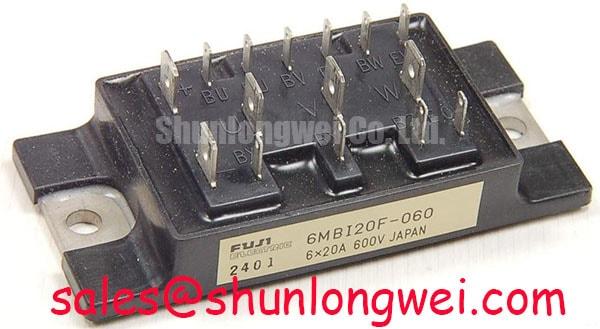
With the DC link discharged and isolated, begin by checking the power terminals of the 6MBI20F-060 for abnormal low resistance, mechanical damage, heat discoloration, loose terminal hardware, or evidence of uneven contact pressure at the heatsink interface. This Fuji Electric IGBT module is rated at 600V VCES and 20A continuous collector current at Tc = 25°C, making accurate verification of the original inverter’s voltage class, terminal arrangement, gate-drive connections, and cooling condition essential before replacement or recommissioning.
The official electrical limits identify a 2.2V typical and 2.7V maximum collector-emitter saturation voltage, along with a freewheel diode forward drop of 2.0V typical and 2.5V maximum. The official total power dissipation rating is 90W, while the maximum specified junction temperature is +150°C. These figures are Official Datasheet Specifications and should be evaluated alongside the complete drive system, including switching frequency, load duty, bus voltage, heatsink condition, airflow, control logic, and protection response.
| Official Specification | Value |
|---|---|
| Manufacturer | Fuji Electric |
| Collector-Emitter Voltage VCES | 600V |
| Continuous Collector Current IC | 20A at Tc = 25°C |
| Collector-Emitter Saturation Voltage VCE(sat) | 2.2V typical, 2.7V maximum |
| Diode Forward Voltage VF | 2.0V typical, 2.5V maximum |
| Total Power Dissipation PC | 90W |
| Maximum Specified Junction Temperature Tj | +150°C |
For device-family context and power-semiconductor reference material, consult Fuji Electric Power Semiconductor & IPM Modules. The module should be treated as one element of a larger inverter power stage rather than as an isolated repair item. A successful return to service depends on confirming the surrounding gate-driver board, DC-link capacitors, snubber network, motor cable condition, current-sensing path, cooling assembly, and fault-history evidence.
Before energizing an inverter fitted with the 6MBI20F-060, compare the motor cable route and output hardware against the original machine configuration. Long motor leads can behave as transmission lines during fast switching edges. A mismatch between cable impedance and motor terminal impedance can reflect energy back toward the inverter, producing terminal overshoot that can approach twice the DC-link voltage under unfavorable conditions. This is a system-level transient effect, not an official voltage allowance for the module.
A dv/dt reactor and an output sinusoidal filter solve different problems. A reactor is generally evaluated where the immediate goal is to moderate edge rate and reduce stress from cable-related reflections. A sinusoidal filter is usually evaluated when the motor must receive a more sinusoidal waveform and the application’s cable, motor insulation, acoustic, or bearing-current conditions justify that approach. The appropriate choice depends on inverter carrier frequency, motor parameters, cable construction, cable length, braking duty, and measured phase-to-phase and phase-to-ground waveforms.
During a site inspection, first confirm that the output conductors are correctly terminated, phase order is preserved, shield bonding follows the machine design, and no output reactor or filter has been bypassed during a previous repair. Inspect the motor cable for crushed sections, fluid ingress, damaged braid termination, and loose cabinet glands. These conditions can alter the output path and complicate diagnosis. An oscilloscope measurement at the inverter output and motor terminals, made with suitable high-voltage differential probing, gives more useful evidence than assuming that an overcurrent trip originates in the IGBT module.
Design Consideration: keep the DC-link capacitor connection and inverter power loop physically compact to reduce parasitic inductance, particularly where turn-off current can create inductive overshoot. The system engineer should verify peak collector-emitter voltage against the DC-link voltage during representative switching and regeneration tests. Clearance, creepage, cable routing, filter bonding, and enclosure grounding should remain consistent with the equipment’s original voltage category and applicable installation requirements.
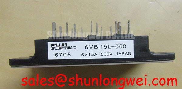
In compact industrial inverters and high-speed CNC spindle drives, deceleration can return energy to the DC link. Confirm that the braking chopper, braking resistor, wiring, and thermal protection are functioning before attributing rising DC-bus events to the 600V module. A failed braking path, excessive inertia, or an incorrect deceleration setting can raise bus stress independently of the output filter decision. Where a related lower-current power-stage position must be checked against its own documented terminal and electrical requirements, the 6MBI15L-060 can be reviewed as a separate Fuji Electric module reference.
Field Diagnostics & Commissioning: Auxiliary Emitter Return Trace Separation in 6MBI20F-060 Topologies
Gate-drive instability is often investigated too late. Before applying full bus voltage, inspect the gate-driver board, plug connectors, control supply rails, isolation barriers, and return-path routing. Do not assume an auxiliary emitter or Kelvin-emitter connection is available on this specific module without verifying the original equipment schematic and the module terminal documentation. If the inverter design provides a dedicated gate-driver return reference, it should remain separated from the high-current emitter return path as intended by the original design.
When a gate-driver return shares inductance with a large switching-current path, the voltage developed across that common path can alter the gate-emitter voltage seen by the switch. The result may appear as ringing, false turn-on behavior, irregular current waveforms, or nuisance protection events. These observations are not a single-cause diagnosis. Check them against gate-emitter waveforms, collector-emitter waveforms, and the known-good phase path where available.
Engineering Recommendation: route the drive loop so that the outgoing gate path and its designated return path remain closely coupled, while keeping that loop away from high-current commutation conductors. This principle helps limit common impedance coupling during switching. The final routing, gate resistance, driver supply bias, desaturation threshold, blanking interval, and any turn-off bias must be determined and validated by the system designer because the official specifications listed for this module do not define those drive-system values.
Where multiple power modules are used in parallel, static current sharing requires careful assessment rather than a visual assumption of symmetry. The temperature behavior of IGBT saturation voltage can support current balancing in appropriate operating regions, but module-to-module matching, busbar geometry, gate-drive timing, thermal paths, and dynamic switching behavior still determine the actual result. Equal physical conductor length alone does not confirm equal electrical impedance. Compare voltage drop, temperature distribution, gate signals, and current measurements across parallel paths during controlled commissioning.
The 2.2V typical VCE(sat) value is useful for understanding the specified conduction characteristic, but it is not a universal field pass or fail reading. A static multimeter check cannot reproduce the operating current, junction temperature, drive voltage, and switching environment represented by a datasheet test condition. Use cold testing to identify obvious shorts or abnormal junction behavior, then use controlled waveform and thermal measurements to assess the assembled inverter.
⚠️ Field Alert: Isolate and discharge the DC link before removing gate or power connections, then reinstall every power fastener and control connector using the equipment manufacturer’s documented assembly method.
When comparing module families for an existing service design, a higher-current part number such as 6MBI100L-060 should not be treated as an automatic substitute. Voltage class, current class, package dimensions, terminal positions, driver compatibility, thermal interface, protection calibration, and the original controller’s operating limits must all be verified from documentation and direct measurements.
Assembly Integrity & Layout Architecture: High-Altitude Cosmic Ray and SEB Considerations for 6MBI20F-060
For equipment operated above 2000m, record the actual installation altitude, DC-link operating range, cabinet temperature, cooling performance, and switching duty before making reliability decisions. Atmospheric neutron flux changes with altitude, and semiconductor susceptibility to single-event effects is a specialized reliability topic. No official FIT rate, single-event burnout rate, altitude derating curve, or cosmic-ray qualification figure is stated in the supplied specifications for the 6MBI20F-060. It would therefore be inappropriate to assign a numerical failure prediction or a mandatory voltage derating value to this model.
Design Consideration: at elevated altitude, the system team should evaluate the complete electrical and environmental design, including actual DC-bus peak voltage, transient voltage at the module terminals, enclosure cooling, insulation coordination, contamination level, protection response, and required regulatory obligations. The objective is to maintain verified operating margin under the real conditions of the equipment, rather than applying an unsupported universal adjustment.
In field service, distinguish between evidence and assumption. A module found shorted after a high-altitude installation may have experienced a transient, a gate-drive fault, inadequate cooling, braking malfunction, output cable event, contamination, or another system condition. Preserve fault logs where available. Inspect the DC-link capacitors, suppression components, control board, motor leads, and grounding system before replacing only the power module. This process improves the chance of identifying the initiating condition without claiming a single failure mechanism.
Physical layout remains relevant because terminal overshoot is influenced by the commutation loop. Laminated bus structures or short, broad, closely coupled conductors are commonly evaluated to reduce loop inductance where switching-current paths are demanding. This is an Engineering Recommendation, not an official package requirement for the module. The system engineer should confirm the result with measured switching waveforms under the actual load and bus-voltage conditions.
For broader discussion of voltage-class and power-conversion technology choices, engineers can review The 1200 V CoolSiC™ MOSFET Advantage in Three. That technical reference does not change the official 600V rating or other published characteristics of the Fuji Electric 6MBI20F-060; it can support a wider system-level review where topology, voltage class, and switching technology are being assessed.
Transient Dynamics & Electrical Design: Thermal Paste Degradation Prevention and Mounting Control for 6MBI20F-060
Remove the old thermal interface material completely and inspect the heatsink contact surface before mounting the replacement module. Dried paste, embedded debris, corrosion, raised burrs, warped surfaces, or uneven residue can create localized thermal resistance. The 90W total power dissipation rating is an Official Datasheet Specification, but actual heat removal depends on the installed heatsink, airflow, interface condition, mounting pressure, ambient environment, and operating cycle.
Apply thermal compound as a thin, continuous, uniform interface layer according to the equipment documentation and the material supplier’s instructions. A thickness in the general range of 50 to 100µm is a Design Consideration commonly used for controlled power-module interfaces, not an official requirement for this Fuji Electric part. The purpose is to fill microscopic surface irregularities without creating an unnecessarily thick insulating layer. The correct process depends on the flatness of the heatsink and module base, paste viscosity, fixture method, and specified mounting hardware.
Use a staged and cross-pattern tightening sequence where the mechanical design has multiple mounting points. This helps distribute clamping pressure across the contact surface and reduces the risk of tilting the module during assembly. Mounting torque must follow the original equipment documentation and the fastener specification. Do not infer a torque value from another package or another manufacturer’s module, since screw size, baseplate construction, thread engagement, washer arrangement, and heatsink material can differ.
After mechanical installation, examine the power terminals and control terminals for correct seating and strain relief. High-current conductors should not place side load on terminals, and gate-drive leads should be routed to avoid coupling into power conductors. Where a bootstrap supply is part of the original gate-drive design, verify its capacitor, charging diode, isolation arrangement, and control-supply behavior against the original circuit documentation. Repeated high-frequency charging, diode recovery behavior, or a weakened auxiliary supply can affect driver operation even when cold resistance tests on the module appear acceptable.
Commission in controlled stages. Verify control supply stability, absence of unintended gate signals, phase-path symmetry, cooling fan operation, and protection functions before applying normal mechanical load. During early operation, monitor heatsink temperature trend, DC-link behavior, motor current balance, and switching waveform quality where test access is available. The official +150°C maximum specified junction temperature is a device limit, not a recommended continuous operating target. Actual junction-temperature assessment must be based on the system’s thermal model and validated operating measurements.