

Content last revised on September 10, 2026
Dynamic Gate Impedance Control for Robust Phase-Leg Dead-Time Operation
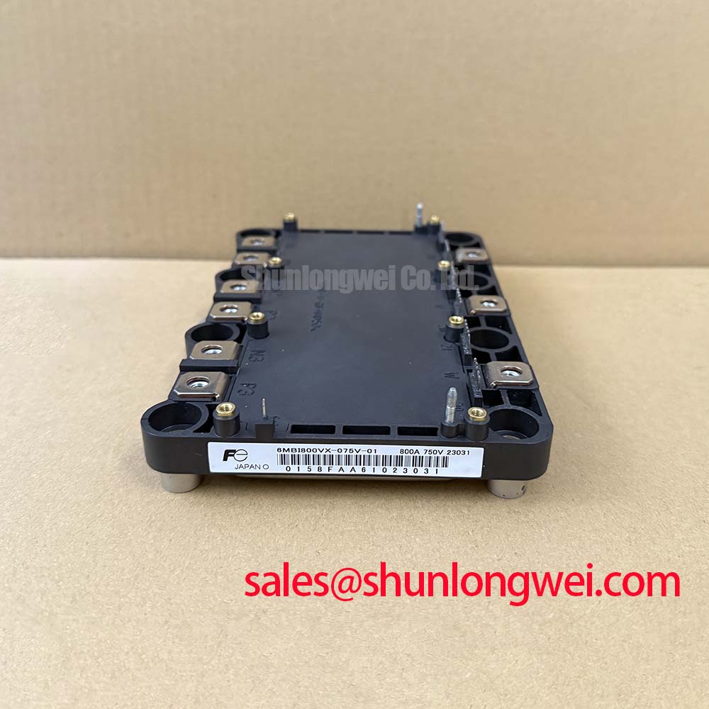
In high-power centralized solar photovoltaic conversion topologies, phase-leg shoot-through represents a catastrophic failure mechanism. The 6MBI800VX-075V-01 from Fuji Electric is a six-pack IGBT module featuring a continuous collector current rating of 800A and a collector-emitter breakdown baseline of 750V (Official Datasheet Specification). Operating this power stage within high-speed switching environments requires meticulous management of dynamic gate impedance to suppress parasitic turn-on induced by severe collector-emitter voltage transients (high dv/dt).
When an opposing switch in a bridge arm commutates rapidly, the resulting dv/dt across the non-conducting IGBT forces a displacement current through its internal collector-gate feedback capacitance (Miller capacitance, Cres). If this current encounters elevated impedance in the gate drive circuit, the gate-emitter voltage can easily exceed the device's threshold voltage (VGE(th)), causing uncommanded cross-conduction. To prevent shoot-through under steep switching gradients, engineers must implement a dedicated low-impedance turn-off path combined with a negative gate bias voltage, typically selected between -5V and -15V (Typical Starting Point for bench tuning).
Active Miller clamping circuits provide a direct, dynamic hardware mitigation technique. By deploying an auxiliary clamping transistor directly adjacent to the module gate-emitter terminals, the gate potential is held low via a shunt path with minimal resistance as soon as the drive signal falls below a predefined threshold (such as 2.0V). This eliminates the reliance on the primary turn-off gate resistor (RG(off)) to sink the displacement current. Furthermore, selecting asymmetrical gate resistors allows fine-tuning: a higher RG(on) limits turn-on peak currents and electromagnetic emissions, while a lower RG(off) preserves dead-time margins and prevents cross-conduction.
💡 Pro Tip: Suppressing gate-loop stray inductance requires routing the gate and auxiliary Kelvin emitter connections as tightly coupled differential microstrip pairs on the printed circuit board, with total loop lengths strictly held under 50 mm. Inserting a low-inductance ceramic bypass capacitor directly across the driver DC supply pins prevents transient voltage sag during rapid gate-charging intervals.
Dead-time allocation must accommodate propagation delays, optical signal dispersion, and temperature-dependent IGBT turn-off fall times (tf). In a 750V, 800A power block, insufficient dead time leads to direct DC-link short circuits, whereas excessive dead time induces severe body-diode conduction losses and output waveform distortion. Bench validation requires monitoring VGE and VCE simultaneously under maximum junction temperature conditions to verify that the spurious gate voltage bounce never approaches VGE(th) throughout the entire load profile.
| Parameter | Datasheet Specification | Engineering Significance |
|---|---|---|
| Collector-Emitter Voltage (VCES) | 750V | Optimized electrical margin for sub-bus segments in solar conversion systems. |
| Continuous Collector Current (IC) | 800A | High power density in a consolidated 6-pack module configuration. |
| VCE(sat) (typ. at TC=25°C) | 1.65V | Low conduction losses, reducing heatsink volume and thermal strain. |
| Isolation Voltage (VISO) | 2500V AC (1 min) | Ensures reinforced galvanic isolation against baseplate and chassis. |
Optocoupler vs Digital Coreless Transformer Isolation in High-Voltage Switching
Galvanic isolation within utility-scale solar inverters must decouple the sensitive digital controller from the high-voltage power stage while withstanding continuous electrical stress. In systems using modules like the 6MBI800VX-075V-01, the gate isolation barrier is subjected to fast ground-potential shifting during switching transitions. The critical parameter determining signal fidelity across this boundary is Common-Mode Transient Immunity (CMTI).
Traditional optocouplers rely on internal LED-to-photodiode optical paths. While offering established high-voltage insulation, optocouplers typically suffer from limited CMTI (often constrained below 50 kV/µs) and parameter drift caused by LED degradation over prolonged operational lifetimes at elevated ambient temperatures. When transient displacement currents breach the parasitic barrier capacitance of an optocoupler, false logic states can be registered at the secondary gate output, triggering spurious conduction. In contrast, modern digital isolators based on coreless transformer or capacitive coupling technologies achieve CMTI ratings exceeding 100 kV/µs to 150 kV/µs, maintaining logic integrity under extreme switching gradients.
The freewheeling diode integrated within each switch must also clear reverse recovery charges rapidly to protect the active semiconductor elements. The underlying physics governing these PN and barrier junctions dictates that low forward voltage drops minimize conduction overhead, a principle also highlighted in studies of semiconductor charge transport such as Schottky barrier physics. Digital coreless transformers provide symmetric, ultra-low propagation delay skew (typically under 10 ns), allowing tighter system dead-time calibration than standard optocouplers could safely support.
Layout clearance and creepage distances along the driver PCB must adhere to reinforced insulation standards (such as IEC 61800-5-1). Engineers must enforce an isolation barrier slot of at least 8 mm to 10 mm beneath the digital isolator IC on the PCB to prevent surface tracking in dusty or humid field installations. High-frequency common-mode chokes should be placed on secondary power supply feeds to suppress residual high-frequency circulating currents between control reference planes and the floating emitter nodes.
Derating Guidelines and Mismatched Parameter Compensation in Parallel Operation
Achieving multi-megawatt capacity in centralized solar arrays frequently demands connecting multiple power stages or entire converter sub-units in parallel. When deploying the 6MBI800VX-075V-01, matching static and dynamic current sharing is essential to maintain junction temperatures (Tj) within conservative operational margins, preventing localized thermal overload.
The positive temperature coefficient of VCE(sat) exhibited by this 750V module (typ. 1.65V at 25°C, increasing predictably at higher junction temperatures) serves as an inherent self-balancing mechanism for static current distribution. As one parallel IGBT channel carries a larger proportion of steady-state current, its die temperature rises, causing its internal saturation voltage to increase. This higher VCE(sat) naturally redirects current into the cooler, parallel modules. However, relying strictly on this thermal feedback is insufficient for dynamic switching intervals.
Dynamic current mismatch arises primarily from discrepancies in gate-emitter threshold voltage (VGE(th)) and unaligned loop inductances. A device with a lower VGE(th) turns on earlier and turns off later, absorbing a disproportionate share of switching energy during each cycle. To compensate for these differences:
- Individual Gate Resistors: Always drive parallel devices using dedicated gate resistors for each module to decouple gate oscillations, rather than tying gates together directly.
- Symmetrical Busbar Geometry: Ensure that the AC and DC busbar paths present identical stray inductances and resistances to every parallel branch.
- Thermal De-rating Factors: Apply a current derating factor of 10% to 15% (Typical Starting Point for engineering calculations) across parallel groups to account for unavoidable manufacturing tolerances and PCB layout asymmetries.
For systems operating at different DC bus levels or requiring distinct switch arrangements, designers frequently evaluate alternative module configurations. For example, high-voltage converter topologies may utilize the 6MBI450V-170 to satisfy 1700V breakdown requirements, while single-switch building blocks such as the 1MBI800UB-120 accommodate discrete phase-leg topologies needing 1200V ratings. Matching the appropriate voltage class to the system architecture prevents excessive silicon cost while retaining adequate breakdown margin.
DC-Link Capacitance Bank Layout and Low-ESL Busbar Interconnection Techniques
During turn-off transitions, the 800A collector current in the 6MBI800VX-075V-01 drops at high di/dt rates. Any parasitic inductance (Lσ) within the DC-link interconnection loop induces an overvoltage spike that adds directly onto the DC bus voltage. The total peak voltage across the switch follows the relationship where the transient surge equals the static DC voltage plus the product of total stray inductance and the rate of current decrease (Vpeak = VDC + Lσ × di/dt). To preserve the 750V rating of the module, parasitic loop inductance must be constrained, typically targeting Lσ < 25 nH across the primary commutation path.
Achieving this low inductance demands planar, laminated busbar architectures. By sandwiching wide copper positive and negative plates separated by a thin dielectric insulator (such as Mylar or Kapton sheets of 0.5 mm to 1.0 mm thickness), the magnetic fields generated by opposing currents cancel each other out, drastically lowering Equivalent Series Inductance (ESL). DC-link film capacitor banks should be distributed symmetrically across the busbar rather than concentrated at a single point, ensuring uniform current distribution and preventing hotspot formation.
Mounting and thermal assembly practices dictate long-term physical reliability. Standard mechanical practice requires applying a uniform layer of high-performance thermal interface material (TIM) with a calibrated thickness of 50 µm to 100 µm across the module baseplate (General Industry Design Consideration). Fastening the module to the liquid cooling plate or heatsink must follow a cross-pattern torque sequence, typically reaching an initial pre-tightening torque of 1.0 N·m followed by a final tightening torque of 2.5 to 3.5 N·m for M5 mounting hardware.
For thorough diagnostic testing, dielectric withstand verification, and structural reliability assessments, engineering teams can consult procedural guides such as the Field Engineer’s Handbook for standardized failure analysis and non-destructive bench validation steps. Verifying low loop inductance, adequate thermal dissipation, and controlled gate transitions ensures that the power semiconductor operates reliably within designated electrical margins throughout its deployment.