



Content last revised on September 14, 2026
7MBR50NF060 Operational Boundaries: Evaluating Active Miller Clamp Implementation Limits
The first bench check should be performed with the module completely disconnected from the DC link and gate-drive supply. Measure the external terminal condition against a known-good reference module or the original equipment documentation rather than assigning a pass or fail value from a generic diode test. A cold resistance reading can help identify an obvious short circuit, open connection, or unexpected imbalance, but it cannot verify switching performance or the condition of an internal semiconductor junction.
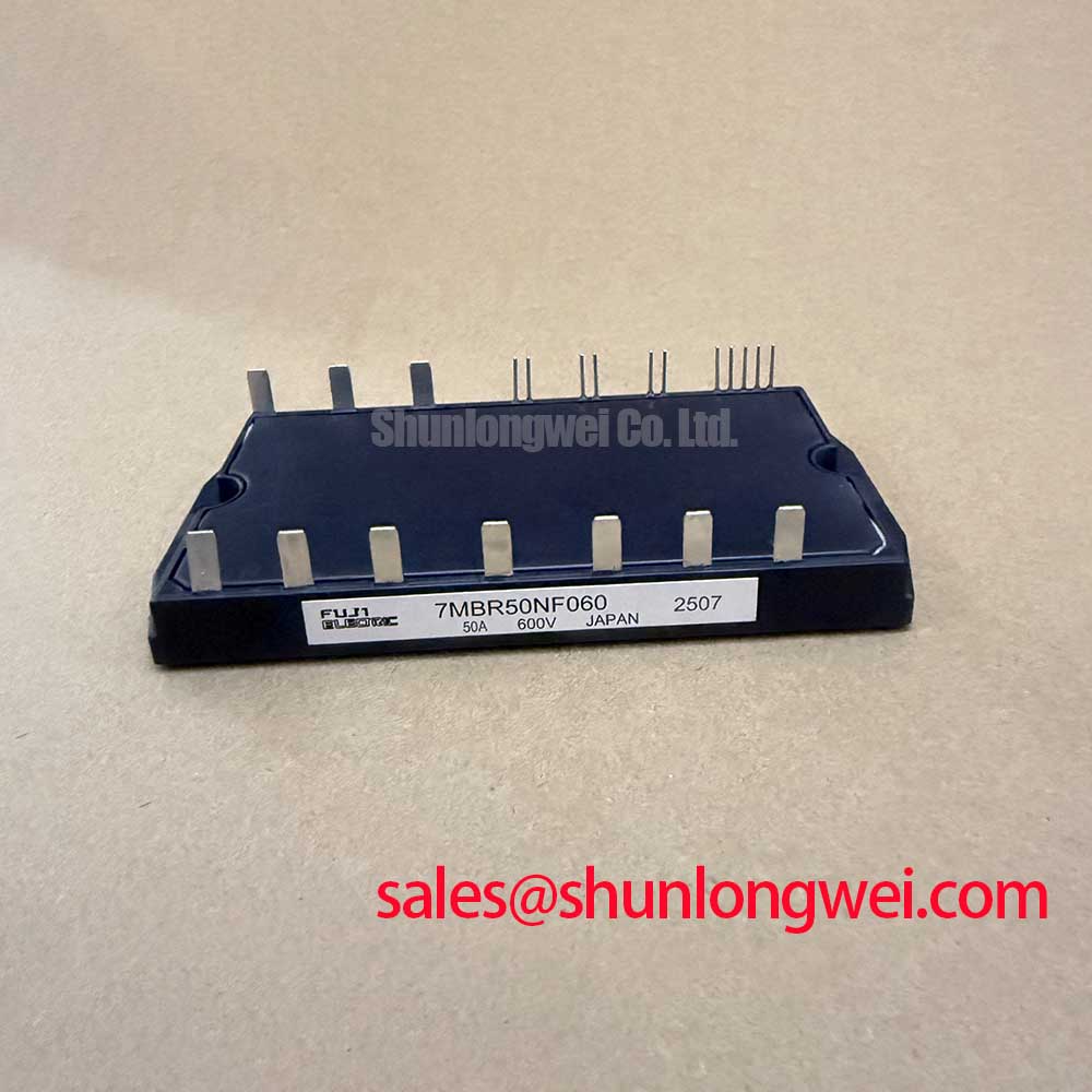
The official identification data supplied for this product gives a 600.0 V rated voltage, a 50.0 A rated current, and a Module package. These are Official Specification values for product identification and initial equipment screening. They do not by themselves establish the permissible DC-link voltage, switching frequency, overload duration, gate resistance, short-circuit withstand, or thermal operating point of a particular drive.
Active Miller clamp evaluation belongs to the complete gate-drive design. During a fast voltage transition on one switching device, parasitic coupling can raise the inactive gate voltage and create unwanted cross-conduction. A dedicated low-impedance clamp path may reduce this risk when the driver, emitter reference, isolation arrangement, and switching loop are designed as one system. The use of negative gate bias is also system dependent and must be confirmed from the applicable Fuji Electric documentation and the installed gate-driver design; it should not be inferred from the module part number alone.
For a field investigation, place the oscilloscope reference at the actual gate-emitter measurement point and use a suitable differential probe. Compare the inactive gate waveform with the known-good phase, then check whether the observed disturbance changes with cable routing, driver supply condition, or busbar configuration. Minimize the gate-loop area and keep the power commutation loop physically separate from sensitive control wiring. The required clearance around high-voltage conductors is determined by the working voltage, pollution environment, insulation system, and applicable equipment standard, so the system engineer must verify it during the layout review.
Fuji Electric provides product information through its Power Semiconductor and IPM Modules resource. For a replacement assessment, compare the original gate-driver interface, terminal arrangement, isolation requirements, and protection functions before applying power.
Assembly Integrity & Layout Architecture: Implementing SCSOA Overcurrent Protection for 7MBR50NF060
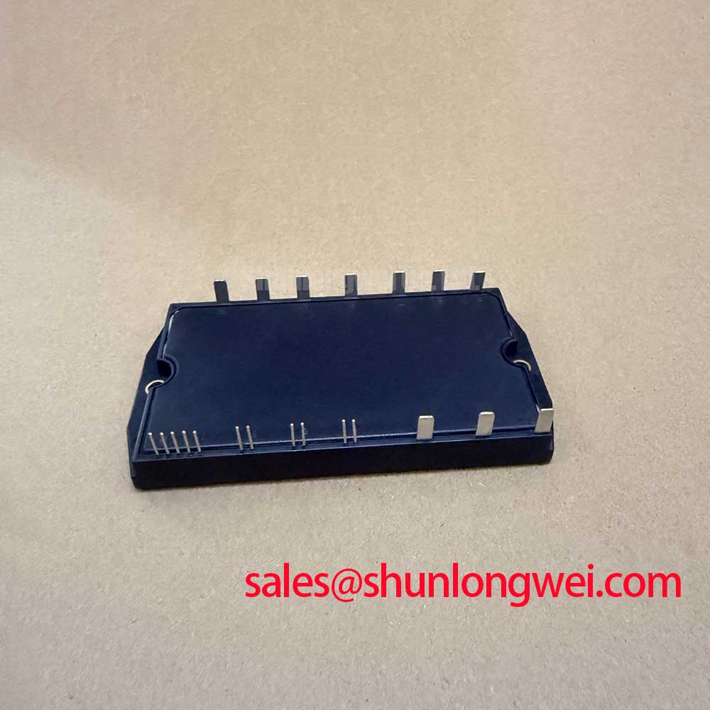
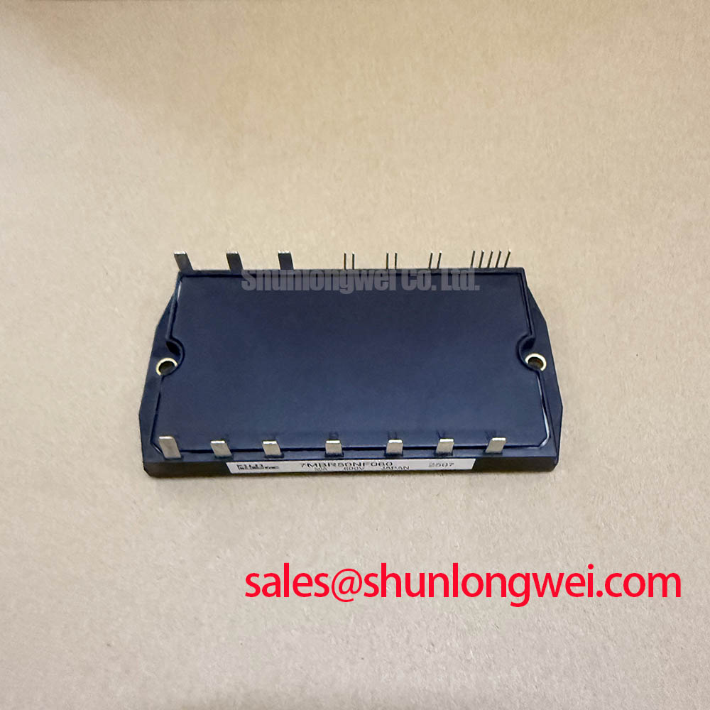
A replacement module should not be installed until the terminal markings, power polarity, auxiliary connections, and mechanical hole pattern have been checked against the equipment drawing. The supplied specification identifies the package only as Module; it does not provide a complete terminal map, internal circuit diagram, mounting dimensions, or short-circuit safe operating area in the available product data. Do not assume that a visually similar module has an identical internal topology or pin assignment.
Short-circuit protection should be treated as a system function. If the drive requires rapid detection and a controlled two-stage soft turn-off, the protection circuit must be validated with the actual current sensor, gate driver, isolation barrier, wiring inductance, and DC-link condition. A target response time, including a response in the microsecond range, must come from the relevant device documentation and the drive safety design rather than from a general PIM category. The turn-off profile should limit gate-drive stress while keeping the switching transient within the voltage capability of the complete power stage.
During fault testing, engineers should capture collector-emitter voltage, phase current, gate-emitter voltage, and driver supply behavior on the same time base. An abnormal waveform may result from sensor delay, driver saturation, wiring inductance, insufficient desaturation blanking, or a damaged module, so the evidence should be compared with a known-good channel. Repeated short-circuit tests without a documented device rating and test procedure can permanently damage the module and should not be used as an informal production check.
Mechanical assembly has a direct effect on electrical reliability. The busbar should sit flat against its mating surface, with fastening that resists vibration without imposing bending force on the module terminals. A laminated or closely coupled busbar can reduce commutation-loop inductance, but the final arrangement must be verified by measuring switching overshoot under the intended current and DC-link conditions. An MOV or another clamping network can be evaluated as part of the overvoltage protection strategy, provided its energy rating, clamping behavior, coordination, and failure mode are reviewed for the complete system.
For thermal mounting, clean both mating surfaces, apply the selected thermal interface material as a uniform thin layer, and follow the equipment manufacturer’s specified fastening sequence. A flat pressure plate or spring washer arrangement may help maintain contact pressure during thermal cycling, but the correct pressure and torque are determined by the module construction, bolt size, heatsink, and assembly drawing. Field Alert: Disconnect the DC link and wait for the equipment discharge procedure to complete before unplugging gate-drive or auxiliary wiring.
When sourcing a physically compatible alternative for engineering review, the 7MBR50LC060 may be compared as a separate Fuji Electric module listing. Compatibility remains subject to verified electrical ratings, internal topology, terminal geometry, gate-drive requirements, and thermal mounting conditions; it should not be treated as an automatic substitute.
Transient Dynamics & Electrical Design: Thermal Time Constants and Peak Junction on 7MBR50NF060
Thermal diagnosis should begin with the complete heat path rather than with the module alone. Inspect the heatsink for contamination, distortion, poor flatness, and blocked airflow. Check that the module base is seated evenly and that the fastening sequence has not tilted the package. Thermal interface material should cover the intended contact area without leaving dry regions or creating a thick insulating layer. The actual junction temperature cannot be established from case temperature alone because transient power, interface resistance, heatsink mass, and airflow all influence the result.
A multi-stage RC thermal model can be used as an Engineering Calculation when the required transient impedance data is available from an authoritative device datasheet. The model applies the power pulse through successive thermal time constants to estimate case and junction response, then compares the calculated peak with the manufacturer’s maximum junction limit. For this product, the available supplied data confirms the 50.0 A rated current but does not provide transient thermal impedance curves, junction-temperature limits, overload duration, or switching-loss tables. Those values must be obtained from the applicable Fuji Electric documentation before numerical thermal margins are calculated.
In the field, record phase current, switching pattern, heatsink temperature, ambient condition, and fault history together. A temperature rise that appears only during acceleration may point toward pulse loading or control behavior, while a rise that remains after the load is removed may indicate inadequate heat transfer or airflow. These observations are diagnostic clues rather than single-cause proof. Compare the affected phase with an equivalent operating phase and verify the measurement method before replacing the module.
Electrical and thermal design are linked through turn-off overshoot. Stray inductance in the busbar and connecting conductors interacts with the rate of current change, so the design principle is to minimize the high-current commutation loop and then verify the measured peak voltage against the system DC-link boundary. Snubber components, MOV networks, gate resistance, switching timing, and busbar geometry should be selected together. No universal component value can be assigned to the 7MBR50NF060 without the drive schematic, operating point, and switching test data.
In a high-dynamics multi-axis CNC or robotics servo evaluation, check whether simultaneous axis activity changes the DC-link ripple or causes regenerative energy to accumulate. The module’s 600.0 V rated voltage remains an Official Specification boundary, not a permission to operate the complete inverter at that voltage under every transient condition. The system integrator should establish voltage headroom using measured waveforms, braking behavior, protective clamping, and the relevant equipment requirements.
For broader measurement methods covering power-module testing and failure analysis, engineers can consult the Field Engineer’s Handbook. It should be used as a technical reference alongside the original equipment service documentation and the applicable component datasheet.
Reliability Considerations: Calculating Failure-in-Time Rates in High-Altitude Applications for 7MBR50NF060
FIT rate, terrestrial neutron effects, Single Event Burnout, altitude derating, and long-term lifetime prediction cannot be calculated responsibly from the product number and the three supplied physical parameters alone. No authoritative FIT table, SEB test report, cosmic-ray qualification record, altitude derating curve, or lifetime model has been provided here for the 7MBR50NF060. Therefore, no numerical failure rate, operating-life claim, burn-out multiplier, or altitude voltage reduction is assigned to this module page.
For installations above approximately 2000 m, treat reduced air insulation strength as a Design Consideration and review the enclosure, creepage, clearance, coating, pollution degree, and applicable safety standard. The required spacing is determined by the working voltage, overvoltage category, material group, altitude correction, and equipment construction. Measure the finished assembly, including busbar edges, screw heads, cable lugs, and contamination paths, rather than checking only the module body.
SEB and cosmic-ray susceptibility are application-level reliability questions requiring manufacturer data and a defined electrical mission profile. The engineering review should collect DC-link voltage, switching conditions, repetitive peak behavior, thermal state, installation altitude, and protection response. If the available manufacturer qualification data does not cover the intended condition, the responsible action is to request clarification or conduct a controlled evaluation under an approved reliability plan, not to infer a FIT value.
When troubleshooting an unexplained high-voltage failure, preserve the failed module, inspect the surrounding clamp network, and document busbar geometry and recorded waveforms before replacing parts. Look for evidence of excessive transient voltage, gate-drive malfunction, loss of thermal contact, contamination, or mechanical loosening. The 600.0 V voltage rating and 50.0 A current rating provide essential identification boundaries, but final suitability depends on the complete inverter design and verified operating conditions.
The 6MBI100L-060 can be reviewed as a related front-end or auxiliary-stage component when mapping the wider power topology. Its presence in the same equipment does not establish electrical interchangeability with the 7MBR50NF060. Engineers should verify the circuit role, ratings, protection coordination, insulation system, and mechanical interface for each position independently.