Content last revised on October 1, 2026
Field Diagnostics and Commissioning for Long Motor Leads
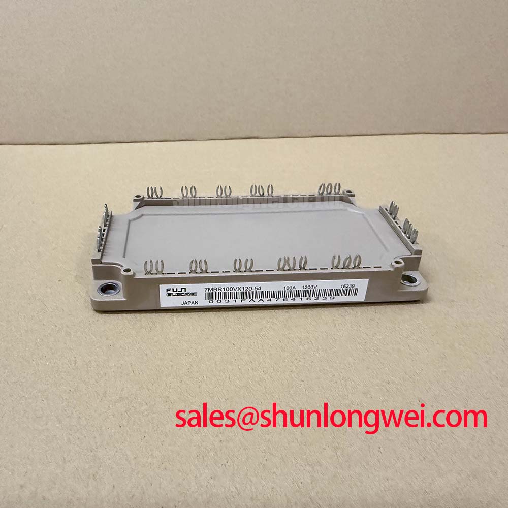
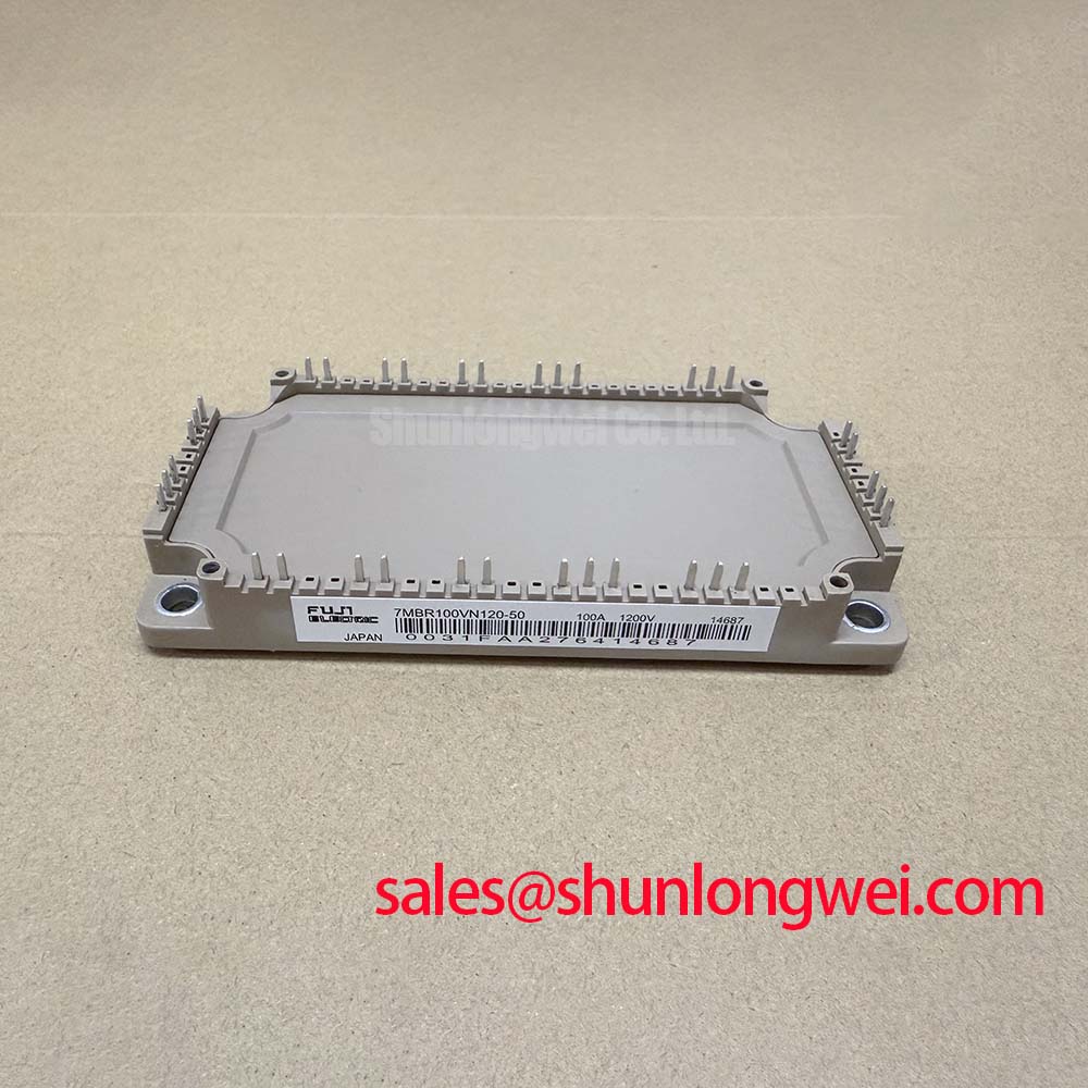
| Manufacturer | Fuji Electric |
|---|---|
| Model | 7MBR109UB120-50 |
| Product Category | PIM Power Module |
| Rated Voltage | 1200.0 V |
| Rated Current | 109.0 A |
| Package | Fuji Power Module |
Measure the switching-node waveform at the power module terminals and at the motor-end cable entry before changing the gate-drive settings. A large difference between these two locations indicates that the cable, termination, and measurement loop are influencing the observed voltage. In a motor drive, long leads can behave as a transmission-line section; impedance mismatch can produce reflected-wave overshoot at the motor terminals and additional stress at the switching module.
The 7MBR109UB120-50 is specified at 1200.0 V and 109.0 A as a Fuji Electric PIM power module. Those ratings identify the module's published electrical class, but they do not define the permissible voltage waveform for every inverter layout, cable length, carrier frequency, or load condition. The system engineer should record the DC-link voltage, switching frequency, motor cable construction, cable length, motor input filter, and measured peak voltage as one test set.
Use a properly rated differential probe with the shortest practical connection at the module terminals. A long probe lead can introduce ringing that resembles a semiconductor fault. Compare the turn-on and turn-off waveforms at no load, rated load, acceleration, deceleration, and fault recovery. The comparison should include the voltage across the module's actual switching terminals rather than relying only on a control-board test point.
A reflected wave may become more pronounced when the cable impedance differs substantially from the source or motor input impedance. The resulting terminal peak can approach a multiple of the local DC-link step in unfavorable conditions. This is a system-level behavior, not a standalone guaranteed characteristic of the Fuji module. Select any output choke, dv/dt filter, or sine-wave filter only after evaluating its effect on switching loss, motor insulation stress, common-mode current, control stability, and fault-clearing behavior.
A practical commissioning sequence begins with a low-energy switching test and a verified current limit. Capture the module-terminal voltage, phase current, gate-emitter voltage, and DC-link voltage on the same time base. If the waveform changes after a filter is installed, check filter resonance and damping rather than treating the improvement at one operating point as a complete validation. The final acceptance test should cover the highest intended DC-link condition and the longest intended motor cable.
Surge suppression should also be coordinated with the DC-link network. A MOV can absorb transient energy, but its clamping behavior, leakage current, thermal loading, and repetitive pulse capability must be matched to the actual bus voltage and fault environment. Place the suppression path so that its current loop does not add avoidable inductance to the commutation path. The MOV is part of the equipment protection network; the 1200.0 V module rating must not be treated as the MOV selection voltage.
Operational Boundaries and PCB Symmetry for Parallel IGBT Paths
Probe the gate-emitter voltage and the power-emitter return at the same time while observing collector-emitter overshoot and phase current sharing. A difference between the auxiliary emitter reference and the high-current emitter reference can expose mutual coupling, common impedance, or an unintended return path that is hidden during static continuity checks.
When a module contains parallel switching paths, the gate-drive layout should preserve electrical symmetry. Keep the gate loop compact, route the gate-drive return with its associated signal path, and separate the auxiliary emitter return from the main high-current emitter connection wherever the terminal arrangement supports that separation. The objective is to prevent load-current voltage from appearing in the gate reference. The exact terminal function and permitted connection method must be taken from the applicable Fuji Electric documentation for this model.
This is a Design Consideration, not an additional factory rating. Unequal copper resistance, unequal trace inductance, or different thermal conditions can cause one path to switch earlier or later than another. Dynamic imbalance may then appear only during high-current transitions. Verify the result with synchronized voltage and current measurements under the intended bus voltage and switching conditions.
Gate-drive sourcing and sinking capability should be selected from the required switching speed, gate charge, driver supply, and acceptable switching loss. The driver must control both positive gate current during turn-on and negative gate current during turn-off without allowing the gate voltage to track a noisy power-emitter reference. An external gate resistor is a Typical Starting Point for bench tuning, not a fixed value for this module. Increase or decrease it only while checking switching loss, collector-emitter overshoot, gate ringing, and current sharing.
Miller coupling deserves specific attention during high-voltage switching. A rapid collector-emitter voltage transition can inject current through the gate-collector capacitance and create a temporary gate disturbance. The preferred design response is a low-inductance gate loop, a controlled turn-off path, appropriate driver sink capability, and a verified clamp strategy where supported by the selected driver. Any negative gate bias, active Miller clamp, or two-level gate resistance must be validated against the driver and the module's documented gate-emitter limits.
For a repair evaluation, compare all parallel gate waveforms against a known-good assembly rather than judging one voltage trace in isolation. Inspect solder joints, busbar pressure, terminal fastening, gate resistor condition, driver isolation components, and local decoupling. A static resistance measurement can identify an open connection, but it cannot establish dynamic current sharing.
Field Alert: De-energize and discharge the DC link before inserting or removing a module connector, gate-drive cable, or measurement lead.
Assembly Integrity and Galvanic Gate-Drive Isolation
Check the isolation barrier with the equipment de-energized, then verify the gate-drive common-mode behavior during a controlled switching test. The measurement should include the isolated power supply reference, driver output, gate-emitter voltage, and switching-node waveform so that a false gate pulse can be separated from probe displacement current or grounding error.
Galvanic isolation is a system design feature involving the driver, isolated supply, printed-circuit-board geometry, connectors, mounting hardware, and enclosure. A reinforced barrier rated above 5 kV and a driver common-mode transient immunity above 100 kV/us may be useful design targets in some high-voltage systems, but these values are not stated factory parameters for the 7MBR109UB120-50. The engineer must select isolation components with ratings appropriate to the working voltage, pollution environment, transient profile, and applicable safety standard.
Maintain a deliberate separation between primary power copper, gate-control circuitry, auxiliary supplies, and accessible metalwork. Creepage follows the surface path, while clearance follows the shortest air path; both depend on working voltage, material group, pollution degree, altitude, coating, and the applicable equipment standard. Do not infer a safe distance from the module's voltage rating alone. Review the complete assembly because a heatsink, mounting screw, cable shield, or test point can reduce the effective isolation path.
Partial discharge is a separate insulation-reliability concern from a simple continuity or dielectric withstand check. Voids, sharp conductor edges, contamination, and uneven field distribution can produce localized discharge activity under repetitive electrical stress. The partial discharge reference provides background on the phenomenon. For a production or qualification program, the test method, voltage profile, acceptance criteria, and equipment configuration should be defined by the responsible engineering and compliance teams.
Thermal assembly also affects electrical reliability. Apply the selected thermal interface material as a consistent, thin coating that covers the intended contact area without contaminating insulation surfaces. The correct layer depends on the material, surface flatness, pressure distribution, and thermal design; it should not be treated as a universal fixed thickness. Confirm the heatsink flatness, mounting-hole alignment, contact footprint, and fastening sequence before applying final torque.
Use the manufacturer's documented mounting instructions whenever available. If the enclosure uses M5 hardware, a mounting torque of 2.5 to 3.5 N·m is a General Industry Design Consideration only and must not replace the module-specific mechanical specification. Uneven fastening can create both thermal resistance and mechanical stress, while excessive torque can damage the base or mounting interface.
For a broader comparison of high-frequency switching tradeoffs, engineers may consult Wide Bandgap Revolution. The article is useful for system-level context, but it does not replace the Fuji Electric data applicable to this silicon power module. Standards and test planning can also be cross-checked through the JEDEC standards resource.
Fault-Clearing Dynamics and Desaturation Protection
Capture the gate-emitter voltage, collector-emitter voltage, phase current, desaturation signal, and driver fault output from the first abnormal transition through gate shutdown. This sequence shows whether the protection circuit is detecting a genuine overcurrent condition, responding to a blanking-window disturbance, or receiving an unwanted signal through the isolated control path.
Desaturation protection is implemented by the gate driver and its external sensing network; it is not an independently stated protection specification of the 7MBR109UB120-50. Type I and Type II protection behavior, detection delay, blanking time, soft turn-off profile, and short-circuit safe operating area must therefore be verified from the selected driver documentation and the module's applicable short-circuit data. A claimed response time below 10 us cannot be assigned to this module without a matching official source and test condition.
During commissioning, use a controlled fault method suitable for the equipment and test laboratory. Record the DC-link condition, gate resistance, driver supply, load current, fault position, and temperature. The protection circuit should turn the device off in a controlled manner while limiting the voltage generated by commutation inductance. The exact two-stage soft turn-off profile is determined by the driver, gate network, busbar geometry, and system energy.
Keep the desaturation sensing path away from high-current commutation conductors and provide the filtering recommended by the driver manufacturer. Excessive filtering can delay detection; insufficient filtering can create nuisance trips during ordinary switching transitions. Check the diode, sense resistor, blanking capacitor, isolated supply, and driver ground reference as a complete network. A fault output without a corresponding power-stage waveform is insufficient evidence for identifying the failed element.
Overvoltage during fault clearing is governed by the DC-link voltage, current at interruption, stray inductance, switching speed, and the available clamp network. Minimize the commutation loop and coordinate the gate turn-off profile with the busbar and snubber arrangement. The engineer should verify peak voltage against the module's 1200.0 V rating under the worst intended operating condition, including supply tolerance and regenerative energy.
The 7MBP150RA120-14 can be reviewed as a neutral reference when assessing a preceding rectifier or auxiliary power stage in the same equipment. It is not a substitute recommendation for the Fuji Electric module. For a lower-current comparison within the same broad voltage class, engineers may also examine 7MBR75U4B120 while checking topology, terminal arrangement, thermal limits, gate requirements, and mechanical compatibility independently.
After a protection event, inspect the module, gate resistor, driver output stage, clamp components, busbar connections, and current sensor before repeating the test. A module that passes a low-energy static check may still show abnormal dynamic leakage, switching asymmetry, or gate disturbance under operating voltage. The final repair decision should be based on measured waveforms and documented electrical and mechanical compatibility.