Content last revised on September 24, 2026
7MBR75U4B120 Operational Boundaries: Evaluating Dynamic Power Loss Dissipation and Multi R Limits
For a failed industrial inverter welder or medium frequency induction heating supply, begin with a cold electrical comparison against a known good assembly whenever one is available. Check for unexpected low resistance between the main power terminals, then inspect the gate control path and emitter return for contamination, cracked solder joints, loose hardware, or evidence of thermal stress. A cold resistance check is a screening method only; it does not prove that the switching junctions, gate insulation, or dynamic behavior are healthy.
The 1200.0 V rating defines the voltage class for application assessment, while the 75.0 A rating identifies the stated current class. Actual operating capability remains dependent on switching frequency, pulse duration, case temperature, cooling design, current waveform, commutation conditions, and the limits specified in the applicable Fuji Electric documentation. Designers should verify conduction loss and switching loss from the complete electrical data before calculating a heat sink or overload boundary.
For pulsed equipment, junction temperature should be assessed through the complete thermal path rather than by using the case temperature alone. An engineering calculation may use the applicable junction to case transient thermal impedance together with the measured pulse profile and cooling conditions. The resulting estimate should be checked against the manufacturer’s permitted junction temperature and the system’s measured case temperature during the real operating cycle. If those thermal impedance curves are unavailable for the exact configuration, the result should be treated as an engineering estimate rather than an official operating guarantee.
Thermal troubleshooting is more reliable when electrical and mechanical checks are performed together. Confirm that the mounting base is clean and planar, that the heat transfer interface is applied consistently, and that clamping force follows the applicable hardware and manufacturer instructions. Inspect the power bus for discoloration and looseness, because an unintended increase in connection resistance can produce local heating that is not visible in a simple no load test.
Field Alert: Disconnect all power sources and allow the DC link to discharge before removing the module or touching gate wiring.
When reviewing a possible alternative, compare voltage class, current class, package geometry, terminal arrangement, gate characteristics, thermal data, and protection behavior line by line. The 6MBI100S-140 may be assessed as a separate replacement option only after the equipment designer confirms electrical, mechanical, and control compatibility; it should not be treated as an automatic substitute for this Fuji Electric module.
Transient Dynamics and Electrical Design: Derating Guidelines and Mismatched Parameters on 7MBR75U4B120
In a high current switching bridge, symmetrical gate wiring is a practical design consideration. Gate and emitter paths should be routed so that each switching position sees comparable loop impedance and a controlled return path. Differences in stray inductance can cause unequal switching speed, ringing, or apparent current imbalance even when the command signals are identical. The correct layout is system dependent and should be verified with an oscilloscope at the actual module terminals.
Static current sharing can benefit from the positive temperature coefficient commonly associated with IGBT conduction voltage in a parallel arrangement, but that general behavior must not be used as a substitute for device specific data. Designers should verify the relevant conduction characteristics over temperature and current, then assess tolerance, thermal coupling, bus impedance, and switching timing. Dynamic sharing is governed by the complete gate loop, driver output impedance, propagation delay, and commutation layout.
Gate driver sourcing and sinking capability should be selected from the actual gate charge, switching time target, driver supply arrangement, and permitted gate voltage range in the manufacturer’s documentation. A larger driver current does not automatically produce a safer circuit. Excessive switching speed can increase voltage overshoot and common mode disturbance, while insufficient drive strength can increase switching loss and heating.
External gate resistance is best treated as a tuning element. A typical starting point may be selected from the confirmed gate charge and the driver’s peak current capability, then adjusted during double pulse or representative system testing. The final value should suppress ringing without creating unacceptable switching loss. The engineer should observe gate to emitter voltage, collector to emitter voltage, and current transition together, rather than choosing resistance from a single waveform.
Soft turn off and desaturation protection require particular care. If the driver detects an abnormal collector emitter voltage, the protection circuit should reduce current in a controlled manner while limiting the stress created by stray inductance. The actual desaturation threshold, blanking interval, fault response, and gate clamp arrangement must come from the selected driver design and its documentation. They are not confirmed product parameters for the 7MBR75U4B120 from the data supplied here.
When the module is evaluated for an inverter welder or induction heating power stage, verify the complete commutation loop under the highest expected bus voltage and current. Minimize parasitic loop inductance as a layout principle, then confirm peak voltage margins through instrumented switching tests. The Fuji Electric Power Semiconductor and IPM Modules resource provides manufacturer level product context, but the system designer remains responsible for matching the selected gate driver and protection circuit to the exact module data.
7MBR75U4B120 Thermal Electrical Optimization: Atmospheric Neutron Radiation Impact on Practical Tuning
High altitude and atmospheric radiation require a qualification discussion, not an assumed failure rate. Neutron related single event effects, including possible single event burnout in high voltage power semiconductors, depend on silicon structure, electric field distribution, applied voltage, altitude, environment, duty cycle, and qualification evidence. No FIT value, burnout probability, or operating life estimate should be assigned to this model without an authoritative source applicable to the exact device and application.
For installations above ordinary industrial elevations, the system engineer should request relevant manufacturer reliability information and compare the real DC link operating voltage with the module’s qualified voltage conditions. Voltage headroom should be established from documented derating guidance and verified by testing. It is not technically responsible to convert altitude alone into a guaranteed percentage reduction or a fixed SEB rate.
Practical field work starts with recording the equipment location, DC link voltage, switching waveform, fault history, cooling condition, and operating load. Inspect whether failures occur during startup, regenerative events, short circuit interruption, or steady operation. These observations help separate possible electrical overstress from thermal, gate drive, mechanical, or environmental contributors, but they do not identify a single root cause without waveform and component evidence.
Insulation coordination also requires system level review. Confirm the required creepage distance, clearance, pollution environment, transient overvoltage category, enclosure condition, and contamination control for the complete assembly. The package label alone does not establish the clearance or creepage requirement of the finished inverter. Designers should verify the applicable equipment standard and measure the actual PCB, busbar, terminal, and heat sink geometry.
For technical background on gate loop behavior, switching stress, and control interface considerations, the Precision Gate Drive Design guide can be used as an engineering reference. It should complement, not replace, the exact Fuji Electric electrical and reliability documentation for the selected module.
Field Diagnostics and Commissioning: PCB Symmetry Considerations for Dual IGBT Topologies
During commissioning, separate the high current emitter return from the quiet gate driver reference wherever the module and driver arrangement require that distinction. Mutual coupling through shared copper can create ground bounce, false protection triggering, or an apparent gate voltage error. The correct return strategy depends on the terminal definition and driver topology, so the integrator should confirm the module’s actual terminal map before modifying a PCB.
Use a short, controlled measurement connection when checking gate to emitter voltage. A long oscilloscope ground lead can introduce ringing that is not present in the circuit, while an incorrectly referenced probe can expose the instrument and operator to hazardous common mode voltage. Compare the same measurement points across a known good channel, paying attention to turn on, turn off, fault response, and recovery after a protection event.
Cold testing should include visual inspection, terminal continuity checks, gate resistance comparison, and examination of the surrounding snubber, driver, and current sensing components. If one channel behaves differently, inspect the complete signal path before condemning the module. A damaged driver resistor, cracked isolation component, poor solder joint, or contaminated connector may produce symptoms similar to a semiconductor fault.
Before applying full power, confirm the interlock, precharge, fault reset, cooling system, and current limiting arrangement. The first energized test should use a controlled condition that allows the engineer to observe bus voltage, gate waveform, switching node behavior, and module temperature. Increase operating stress only after the measured waveforms remain within the documented limits for the module and the associated driver.
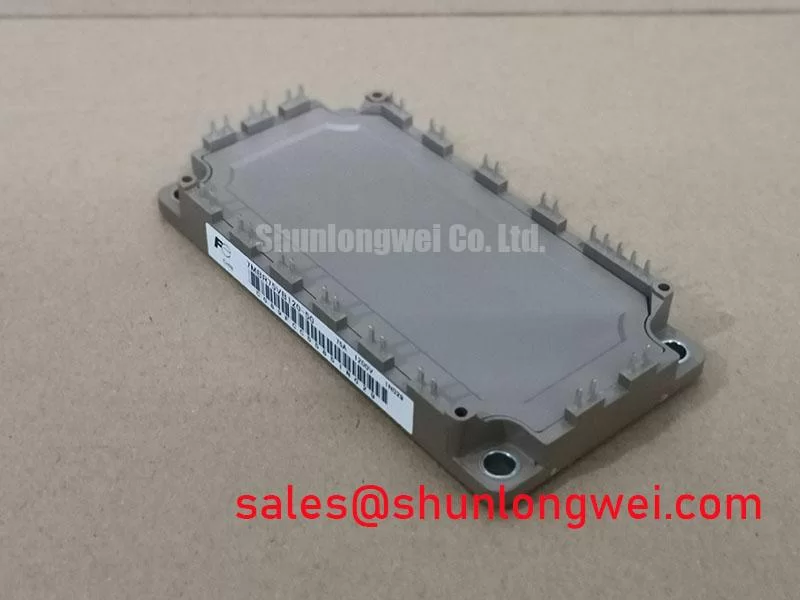
For product context and current manufacturer information, consult the Fuji Electric Power Semiconductors Portal. When purchasing or evaluating a replacement, compare the marked model, official electrical ratings, package requirements, terminal arrangement, and the original equipment documentation before installation. The 7MBR75U4B120 remains a 1200.0 V, 75.0 A Fuji Electric Module whose final suitability must be confirmed against the complete power stage and operating profile.