
Content last revised on September 30, 2026
Incoming Inspection and Identification of 2MBI150U4B-120
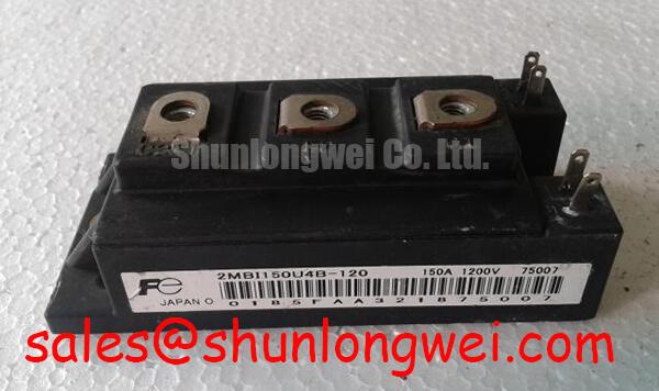
Begin incoming inspection by isolating the device from the gate driver, confirming the marked terminal polarity against the original circuit drawing, and recording cold-state diode-mode readings before applying any control voltage. The 2MBI150U4B-120 is a Fuji Electric IGBT Module specified in the supplied product data at 1200.0 V and 150.0 A, with a Module package classification. These are official product parameters for identification and procurement; switching limits, thermal resistance, gate-charge data, terminal layout, and isolation ratings should be verified from the applicable Fuji Electric documentation before a repair or redesign.
For bench work, inspect the case, power terminals, control terminals, mounting surfaces, and marking condition without energizing the part. Use an ESD-controlled workstation, keep the gate terminal referenced to the emitter during handling, and compare readings with a known-good unit from the same equipment family. A diode-mode reading across a freewheel path can confirm a conductive junction direction, but it does not by itself prove that the insulated gate, die, bond wires, or dynamic switching behavior are healthy.
| Item | Supplied specification | Engineering interpretation |
|---|---|---|
| Manufacturer | Fuji Electric | Use the original equipment documentation to confirm terminal arrangement and application compatibility. |
| Part number | 2MBI150U4B-120 | Match the complete marking before installation. |
| Rated voltage | 1200.0 V | Official supplied parameter; switching overshoot and system transients require separate verification. |
| Rated current | 150.0 A | Official supplied parameter; actual permissible current depends on temperature, switching conditions, duty cycle, and cooling. |
| Package | Module | Mechanical fit, terminal geometry, mounting method, and insulation arrangement must be checked against the host assembly. |
Transient Dynamics and Electrical Design: Static and Dynamic Current Distribution on 2MBI150U4B-120
When this module is evaluated in a commercial string inverter or micro-grid energy-storage converter, the first electrical task is to separate steady-state current sharing from switching-current behavior. The supplied 150.0 A rating is an identification parameter, not a universal operating-current prescription. Designers should verify the current waveform, junction temperature, pulse duration, modulation pattern, and cooling condition at the actual operating point.
For parallel semiconductor paths, the positive temperature coefficient commonly associated with IGBT conduction voltage can support static current balancing because a hotter path tends to develop a higher conduction drop. This is a Design Consideration rather than a guaranteed device-specific sharing curve. The engineer should confirm the behavior with temperature-controlled measurements and should account for differences in gate threshold, conduction voltage, wiring resistance, and thermal coupling between positions.
Dynamic sharing is governed more strongly by the gate and commutation loops. Keep the gate-drive conductors for parallel positions symmetrical in length, routing, return path, and connector contact resistance. Minimize the parasitic loop inductance in the high-current commutation path to reduce turn-off overshoot, then verify the peak collector-emitter voltage with a properly rated differential probe during controlled switching tests. The measured peak must remain within the verified voltage boundary of the system and the applicable device documentation.
A laminated DC-link bus structure can reduce the physical loop area between the positive and negative conductors, while a short connection between the module and local capacitor bank can reduce unwanted voltage excursion. Clearance and creepage must be established from the complete system voltage, pollution environment, insulation scheme, and applicable safety standard; the module’s 1200.0 V supplied rating does not define the required board or busbar spacing.
If two legs show different switching transitions, inspect the gate-emitter reference, driver supply stability, gate resistor population, connector seating, and probe grounding before attributing the variation to the semiconductor. An oscilloscope comparison against the known-good phase is more useful than a single static resistance reading. For a related Fuji Electric device under a replacement study, engineers can review 2MBI150UC-120 as a separate part and then confirm pinout, ratings, and mechanical compatibility rather than treating the two designations as interchangeable.
Preventing Spurious Faults: Evaluating Thermal Capacitance and Heat-Sink Response for 2MBI150U4B-120
Thermal evaluation should begin with the real load profile instead of a nominal current label. In a storage inverter, the module may experience short acceleration of current during peak shaving, regenerative energy transfer, battery charging, or battery discharge. The relevant junction temperature is therefore a time-dependent result of conduction loss, switching loss, case temperature, interface quality, and heat-sink response.
A transient thermal model using junction-to-case and case-to-sink elements can be used as an Engineering Calculation to estimate the temperature rise after a pulsed overload. The model should be populated with verified thermal impedance data from the applicable Fuji Electric documentation. Where a complete multi-RC network is unavailable, treat the result as a screening estimate and validate it with case-temperature measurements, calibrated thermal sensors, and switching-loss tests.
Thermal capacitance matters because a short current pulse may not immediately produce the same case-temperature response as a long-duration overload. This delay must not be interpreted as proof of safe junction temperature. The test plan should capture pulse width, repetition pattern, initial case temperature, coolant or airflow condition, and the interval between load events. Designers should evaluate the converter across its intended switching-frequency range, including low-frequency high-current operation and higher-frequency conditions where switching loss can dominate.
High-ambient operation requires a separate cooling review. Check heat-sink contact flatness, interface material coverage, clamp pressure, fan direction, filter blockage, enclosure recirculation, and sensor placement. Airflow should be verified at the module heat sink rather than assumed from the fan nameplate. A rising thermal baseline between repeated charge and discharge events may indicate insufficient heat rejection, excessive switching loss, poor interface contact, or an inaccurate thermal sensor location; each condition requires measurement.
The Fuji Electric Brake Chopper IGBT Modules reference provides useful industry context for chopper applications, but it should not be used as a substitute for the exact electrical and thermal data of this part. In a service investigation, record the cold resistance and diode-mode behavior first, then inspect the gate waveform and thermal response under a controlled low-energy test. Avoid drawing a failure conclusion from one diode reading because parallel paths, attached capacitors, and circuit topology can influence the result.
Assembly Integrity and Layout Architecture: Dynamic Gate Impedance Control for 2MBI150U4B-120
Gate-loop integrity is a practical fault-prevention measure for any high-current IGBT module installation. The control reference must return to the driver through the intended low-noise path, not through a power-emitter connection carrying rapidly changing current. Common-mode ground bounce can shift the apparent gate-emitter voltage and create false turn-on indications, incomplete turn-off, or protection trips.
Active Miller-clamp circuitry may be considered where the driver architecture and module interface support it. Its purpose is to hold the gate in a controlled off-state during the interval when collector voltage changes rapidly. A negative gate bias may also be evaluated as a Design Consideration, but its polarity, magnitude, transient behavior, and driver insulation must be determined by the system engineer from the verified gate-emitter limits and the complete switching waveform. No negative-bias value should be assumed from the product number alone.
Gate resistance should be treated as a dynamic tuning element. Changing it affects switching speed, electromagnetic behavior, overshoot, driver loss, and Miller interaction. Begin with the value permitted by the validated gate-driver design, then compare turn-on and turn-off waveforms at the module terminals. If a fault appears only at higher load or bus voltage, examine the gate-emitter waveform directly at the module, including the driver return path, rather than measuring only at the controller output.
Keep power and gate wiring physically separated where practical, cross noisy conductors with controlled geometry, and route any clamp or desaturation signal away from the commutation loop. Protection timing must be validated against the actual short-circuit response, driver delay, blanking behavior, and current-sensor bandwidth. The module itself cannot independently claim compliance with system EMC requirements; the assembled inverter must be evaluated against its applicable compliance standard.
💡 Bench Tip: Never connect or remove the gate-drive harness while the DC link or driver supply is energized; discharge the system, apply ESD protection, and repeat the cold-state reference measurements after installation.
The broader Fuji Electric 7th-Gen X-Series IGBT Modules information can help engineers understand the manufacturer’s wider IGBT product context, while compatibility for this specific module still depends on its documented pin arrangement, gate limits, switching data, and mechanical interface.
2MBI150U4B-120 Thermal-Electrical Optimization for High-C-Rate Battery Cycling
In a bidirectional DC-DC stage, the power path reverses as the battery rack changes between charge and discharge. The module may therefore experience different conduction paths, switching states, and thermal distributions during a single operating cycle. The 1200.0 V voltage parameter and 150.0 A current parameter provide a starting point for part identification, but the system designer must verify bus voltage, current direction, switching stress, pulse duration, and temperature for each quadrant of operation.
Thermal swing reduction begins with control of the load profile. Soft transitions, appropriate current slew management, balanced phase operation, and avoidance of repeated operation near the hottest measured condition can reduce rapid temperature movement. These are Engineering Recommendations, not guaranteed lifetime improvements for this individual part. Any lifetime assessment requires authoritative power-cycling data, the exact case-temperature swing, mounting method, mission profile, and a documented reliability model.
During peak shaving, log battery current, DC-link voltage, module case temperature, heat-sink temperature, gate timing, and protection events in the same time record. Correlating these channels can distinguish a thermal accumulation problem from a control-loop event or a commutation overshoot. If the case temperature remains moderate while protection activates, inspect voltage spikes, gate disturbance, current-sensor placement, and desaturation behavior. If temperature rises gradually over repeated cycles, review cooling recovery time and the thermal model assumptions.
Regenerative braking or excess photovoltaic energy may route power through a brake chopper and resistor bank rather than directly into the battery. The external resistor, chopper duty control, DC-link sensing, and fault-interlock sequence must be assessed as one topology. The related 2MBI300U4H-120-50 can be considered as a separate device in an associated rectification or front-end study, subject to independent verification of its ratings and connection requirements.
For engineers building a validation plan, The Ultimate IGBT Knowledge Base offers additional background on IGBT operating principles and structure. Use that material as technical context, while basing procurement and final integration decisions for 2MBI150U4B-120 on the applicable manufacturer documentation and measured behavior in the target inverter or micro-grid energy-storage assembly.