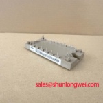
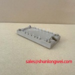
Content last revised on September 10, 2026
High-Frequency Commutation Loop Inductance Minimization in High-Power Arrays
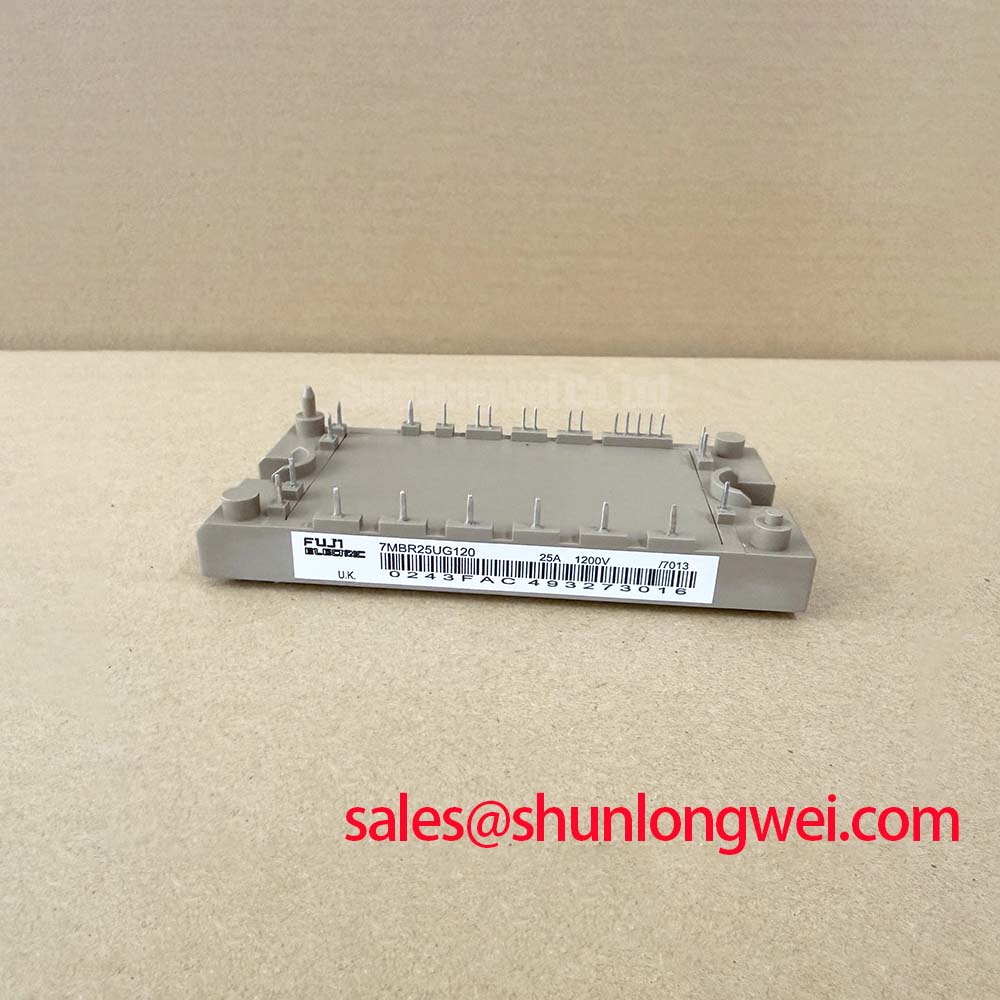
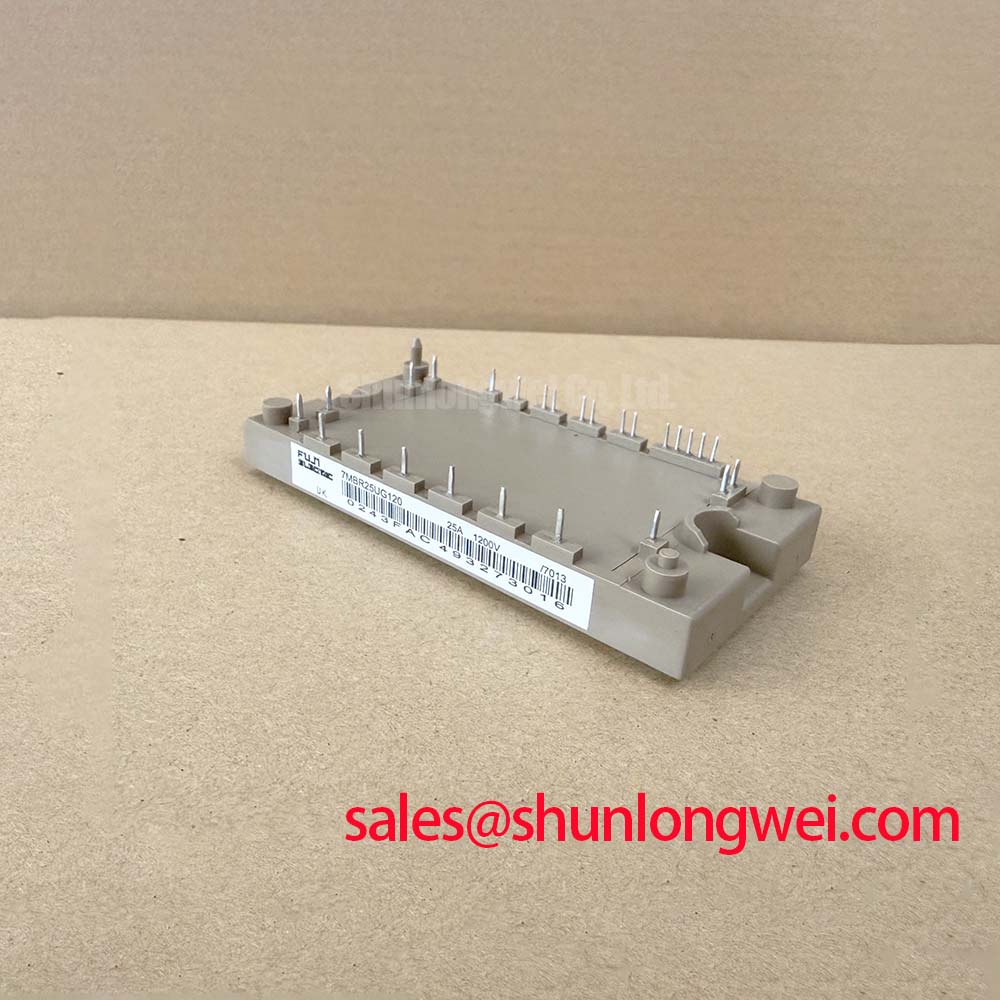
In multi-joint robotic articulator drives and light automation controllers, dynamic switching transients require careful layout geometry to prevent excessive overvoltage stress. When the inverter stage of the 7MBR25UG120 switches off peak inductive currents, the parasitic loop inductance between the DC-link decoupling capacitors and the power silicon induces a transient voltage surge. This transient behavior is governed by the physical interaction where peak collector-emitter voltage equals the instantaneous DC-bus voltage plus the product of total stray loop inductance and the current slew rate. Without adequate attenuation, these spikes risk exceeding the inverter stage rating of VCES = 1200V (Official Specification).
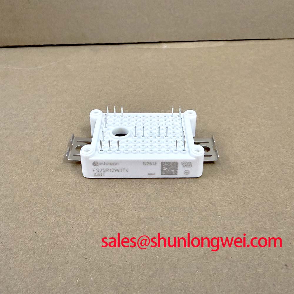
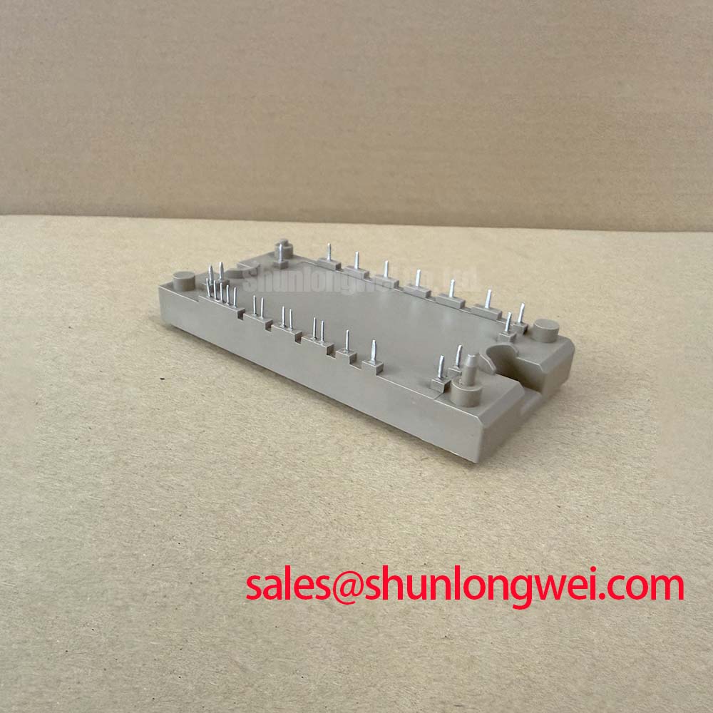
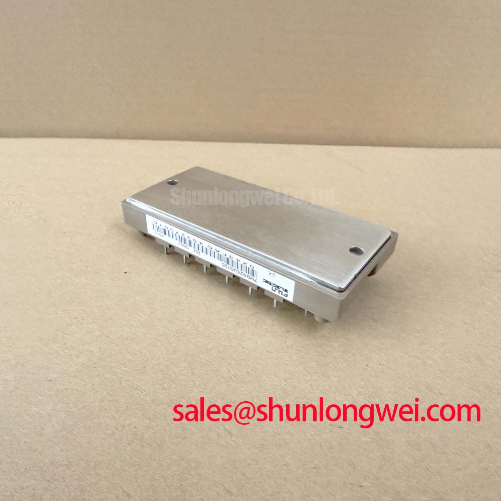
To restrict total loop inductance to under 25 nH (General Industry Design Consideration for compact power modules), layout routing must employ wide, low-profile planar laminated busbars directly interfaced with the module pins. Positioning high-frequency polypropylene film snubber capacitors as close as possible to the DC positive and negative input terminals shunts high di/dt energy locally. For systems evaluating modular layout strategies, comparing integrated Power Integrated Module (PIM) topologies against discrete six-pack arrangements like the 6MBI25F-120 highlights the advantage of the PIM architecture, which houses the three-phase input rectifier, brake chopper, and six-switch inverter in a single housing to minimize physical interconnection loops.
Active Miller Clamp Implementation & Parasitic Capacitive Turn-On Prevention
High-speed pulse-width modulation (PWM) across compact multi-axis servo inverters introduces steep dv/dt voltage transitions across the non-conducting switches. In the 7MBR25UG120, rapid collector-emitter voltage rise forces displacement current through the internal reverse transfer capacitance (Miller capacitance, Cres) into the gate driving circuit. If the gate impedance presents insufficient sink capability, this displacement current creates an unintended voltage drop across the turn-off resistor, potentially lifting the gate potential above the IGBT threshold voltage and precipitating bridge shoot-through.
Implementing a dedicated active Miller clamp circuit provides a direct, low-impedance path that shunts capacitive currents to the emitter line once the gate voltage falls below a preset threshold (typically around +2.0V during turn-off). Alternatively, employing an asymmetric split-rail gate drive with a negative bias voltage between -5V and -15V (Typical Starting Point for bench tuning) provides robust noise margin against dynamic ground bounce. Gate drive impedance calculations can be benchmarked against switching dynamic parameters documented for Fuji Electric High-Speed Discrete IGBTs to verify transient peak current handling across operating temperature ranges.
💡 Pro Tip: Ensure that the gate drive output loop uses a dedicated Kelvin emitter return connection routed directly to the corresponding auxiliary emitter pin. Running gate and emitter traces as tightly coupled differential pairs minimizes mutual magnetic coupling from the high-current output stages.
Galvanic Gate Drive Isolation, Reinforced Creepage & High-CMTI Signaling
Industrial robotic arms operating in noisy factory environments demand robust galvanic isolation between low-voltage digital signal processors (DSP) and high-voltage inverter stages. The Fuji Electric 7MBR25UG120 provides an internal module isolation rating of AC 2500V for 1 minute (Official Specification), establishing the baseline galvanic barrier between active silicon dies and the baseplate heatsink.
To maintain signal integrity during severe electrical disturbances, optocouplers or digital isolators must exhibit a Common-Mode Transient Immunity (CMTI) exceeding 100 kV/μs. Inadequate CMTI allows rapid ground potential shifts to corrupt logic states, resulting in false gate triggering or missing drive pulses. PCB designers must also enforce minimum creepage and clearance distances across the isolation barrier on the carrier board, ensuring compliance with industrial pollution degree standards. When diagnosing unexpected inverter trip sequences or intermittent driver faults during commissioning, standard verification procedures and insulation testing routines should follow the baseline methods detailed in the Field Engineer’s Handbook.
Overvoltage Trip Prevention via Fast-Switching Ballast Chopper Topology
When robotic articulator joints rapidly decelerate high-inertia mechanical payloads, the permanent magnet synchronous motors act as generators, pumping kinetic energy back through the inverter freewheeling diodes into the DC link. Because the input stage uses uncontrolled three-phase rectifier diodes rated at a repetitive peak reverse voltage of VRRM = 1600V (Official Specification), this regenerated power cannot feed back into the AC utility mains, causing the bus voltage to climb rapidly toward overvoltage trip limits.
The 7MBR25UG120 addresses dynamic deceleration through an integrated braking stage featuring a dedicated brake IGBT rated at a continuous collector current of IC = 15A (Official Specification) with VCES = 1200V (Official Specification). Connecting an appropriately sized external power ballast resistor across the dynamic braking terminals allows the controller to activate the chopper switch whenever the DC bus exceeds predetermined thresholds (such as 700V to 750V on a 400VAC line). For multi-axis setups requiring substantially higher regenerative energy absorption beyond compact PIM limits, centralized braking topologies utilizing high-capacity switches such as the 1MBI900V-120-50 offer alternative single-switch architecture options across centralized DC-bus installations.
| Functional Stage | Key Electrical Parameter | Official Datasheet Value | Parameter Classification |
|---|---|---|---|
| Inverter Stage (IGBT) | Collector-Emitter Voltage (VCES) | 1200 V | Official Specification |
| Converter Stage (Diode) | Repetitive Peak Reverse Voltage (VRRM) | 1600 V | Official Specification |
| Brake Stage (IGBT) | Collector Current (IC) | 15 A | Official Specification |
| Module Isolation | Isolation Voltage (Viso, 1 min) | AC 2500 V | Official Specification |