

Content last revised on September 10, 2026
7MBR25SC120-50 Circuit Protection & Reliability: Calibrating Fault-Clearing Dynamics: Type I/II Desat
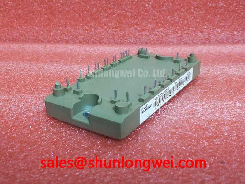
Before reconnecting a drive board, verify the module marking against the service record, inspect the power terminals and case for heat damage, and compare cold resistance readings with an equivalent known-good circuit path where available. The 7MBR25SC120-50 from Fuji Electric is a 1200V, 25A power module. The system integrator should verify the terminal assignment, gate-drive interface, and protection thresholds from the original equipment documentation before installation.
| Parameter | Specification |
|---|---|
| Manufacturer | Fuji Electric |
| Part Number | 7MBR25SC120-50 |
| Voltage Rating | 1200V |
| Current Rating | 25A |
| Package | Module |
For equipment repair, this module should be assessed as part of the complete switching stage rather than as an isolated replacement. DC link capacitors, gate-driver output integrity, current sensing, protection logic, heatsink flatness, and motor cable conditions can all influence measured switching stress. Fuji Electric’s power semiconductor and IPM portfolio provides useful product-family context when reviewing the architecture of an existing power converter.
A desaturation protection circuit should be tested with the actual driver, busbar, DC-link arrangement, and load path used in the repaired equipment. Type I and Type II short-circuit responses are system-level protection concepts, not published operating guarantees for this specific module. In many IGBT driver designs, fault recognition and gate response are evaluated within a sub-10 microsecond window to remain compatible with the applicable short-circuit safe operating area. The final threshold and timing must be verified against the complete converter design.
When a fault is detected, a two-stage soft turn-off approach is commonly evaluated as a Design Consideration. Instead of abruptly collapsing the gate command, the driver controls the removal of gate charge so that inductive overshoot can be limited while the fault path is cleared. This is particularly relevant when a repaired board has changed cable routing, capacitor placement, or busbar geometry. A sudden turn-off event can create a peak collector-emitter voltage above the intended DC-link operating level.
Trace the desaturation sense path separately from high-current switching conductors and confirm that its return reference matches the driver’s intended emitter reference. During troubleshooting, capture the gate-emitter voltage, collector-emitter voltage, and fault output simultaneously. A false trip may indicate noise coupling or an unsuitable blanking sequence, while delayed response may indicate sensing-path or driver-stage degradation. Neither condition should be assigned to the module without waveform evidence.
⚡ Safety Interlock Note: Fully discharge and verify the DC-link voltage before disconnecting gate or power terminals, because stored energy can damage the module and measurement equipment.
7MBR25SC120-50 Operational Boundaries: Evaluating Baseplate Thermal Grease Layer Control Limits
Thermal contact begins with a clean heatsink surface and a baseplate free from residue, burrs, or visible deformation. A thermal interface layer in the 50 to 100 micrometre range is a General Industry Design Consideration, not a Fuji Electric module specification. Its purpose is to fill microscopic surface irregularities without creating an unnecessarily thick thermal barrier. The applicable material, thickness, and mounting procedure must follow the equipment manufacturer’s service documentation.
Mounting screws should be tightened in a controlled cross-pattern sequence so clamping force develops evenly across the baseplate. This helps compensate for normal surface variation and reduces the chance that one portion of the thermal interface is compressed while another contains a void. If the removed module shows localized discoloration or uneven grease transfer, inspect heatsink flatness and cooling-path cleanliness before fitting the replacement.
Dead-time control also deserves attention after installation. Complementary gate commands require an interlock interval sufficient to prevent both switches in a converter leg from conducting simultaneously. This interval is system-determined because driver propagation delay, gate impedance, temperature, and switching behavior all affect the required margin. Verify complementary gate timing at the module terminals under controlled operating conditions rather than relying only on controller firmware settings.
In a converter using separate front-end and inverter functions, technicians may also review related power-stage devices such as the 7MBR50SB120-01 when mapping the wider rectification and switching chain. Electrical compatibility must be established from the original schematic, ratings, pin configuration, and thermal arrangement.
Benchtop Waveform Tuning: Mitigating Stress via Dynamic Gate Impedance Control for Robust on 7MBR25SC120-50
Gate-drive measurements should be made as close as practical to the module gate and emitter references, using a probing method suitable for fast switching nodes. High dv/dt can couple through parasitic capacitances and lift the gate voltage of a device intended to remain off. This may appear as gate ringing, distorted collector waveforms, unexpected current rise, or protection events during commutation.
Dedicated low-impedance turn-off paths and active Miller clamp functions are common Design Considerations where the driver supports them. Negative gate bias is also sometimes evaluated in IGBT converter designs, but its value, driver capability, isolation rating, and gate-voltage limits must be confirmed for the specific system. It should not be assumed from the module voltage and current ratings alone.
Minimize gate-loop and power-loop parasitic inductance to suppress turn-off overshoot, then verify peak voltage margins against the DC-link voltage during double-pulse or controlled switching tests. 💡 Pro Tip: Keep the outgoing and return busbar paths physically coupled and symmetric where practical, then validate the result with measured switching waveforms rather than visual layout judgment alone.
For a current-capacity comparison within the same manufacturer family, the 7MBR35UA120 can be reviewed as a separate engineering reference. It should not be treated as a direct substitute until voltage rating, circuit topology, terminal arrangement, drive requirements, thermal behavior, and protection coordination have been checked.
Transient Dynamics & Electrical Design: Calculating Failures in Time Rates in High-Altitude Service on 7MBR25SC120-50
No Failure in Time rate, single-event burnout rate, service-life figure, or altitude derating value is stated here for the 7MBR25SC120-50, because such claims require applicable manufacturer data or a documented qualification source. Terrestrial neutron exposure, DC-bus stress, enclosure temperature, cooling performance, and switching transient amplitude are all system-dependent variables. A module’s 1200V rating is a specified device rating, but it does not by itself establish a converter’s safe transient margin at a particular altitude.
For installations above 2000m, altitude-related insulation coordination and cooling effects should be evaluated at equipment level according to the governing installation requirements. This is a Design Consideration. Engineers should inspect the complete assembly, including creepage paths, enclosure ventilation, DC-link peak voltage, protection response, and thermal performance under the actual load cycle.
Where resonant or half-bridge behavior is involved, switching-current direction and commutation timing can materially alter device stress. The technical discussion at Resonant Topologies in Home Appliances can support a structured review of waveform behavior, while Fuji Electric’s PIM 7-Pack information offers manufacturer-level context for integrated power-module families. Any final suitability decision should be based on measured electrical and thermal results from the target equipment.