

Content last revised on September 10, 2026
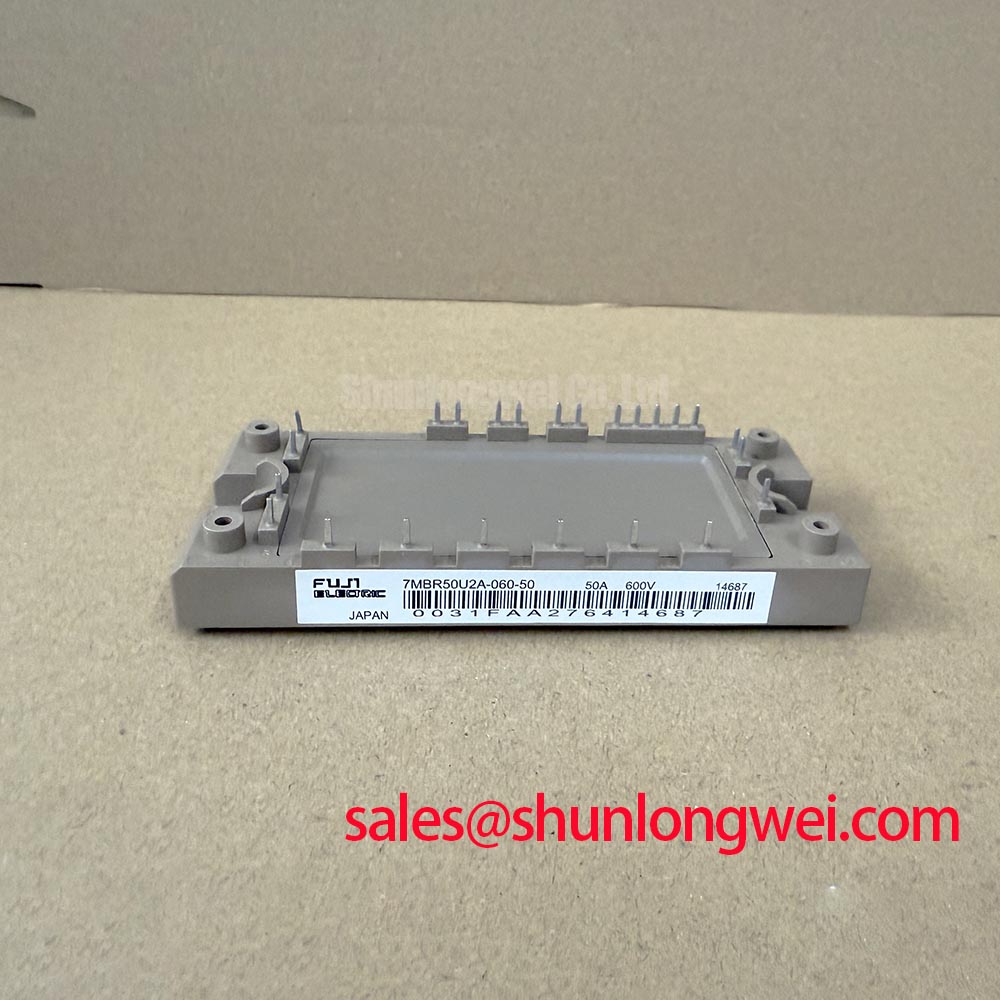
Fuji Electric 7MBR50U2A-060-50 PIM for Industrial Inverter Repair
Before energizing a replacement, isolate the drive, protect the module from ESD, and compare the unpowered terminal arrangement with the original wiring diagram; then verify the marked power terminals and control terminals before applying any test voltage. The 7MBR50U2A-060-50 is a Fuji Electric PIM 7-pack power module intended for inverter power conversion, combining an integrated rectifier, inverter switching devices, and brake chopper functions within one module assembly.
For repair engineers and purchasing teams, the key identification points are its 600 V collector-emitter voltage rating, 50 A inverter current rating at Tc = 80°C, typical Vce(sat) of 1.70 V under the specified test conditions, and maximum stated junction temperature of 150°C. These are official product parameters supplied for this page and should be checked against the original equipment documentation, gate-driver design, cooling arrangement, and operating duty before installation.
| Parameter | Official specification | Engineering significance |
|---|---|---|
| Manufacturer | Fuji Electric | Use the manufacturer identification when matching service records and equipment documentation. |
| Module configuration | PIM, 7-pack | Integrates rectifier, inverter, and brake chopper functions for a compact power stage. |
| Collector-emitter voltage, VCES | 600 V | Provides a voltage class suitable for evaluation in 400 V-class AC input systems, subject to DC-link surge verification. |
| Inverter current, IC | 50 A at Tc = 80°C | Defines the stated inverter current condition; actual usable current depends on thermal resistance, switching conditions, and overload duty. |
| Vce(sat), typical | 1.70 V under the specified test conditions | Useful for preliminary conduction-loss estimation, while the complete loss calculation must include current waveform and switching behavior. |
| Maximum junction temperature | 150°C | Sets the specified upper junction-temperature boundary; it is not a substitute for thermal design verification. |
Benchtop Waveform Tuning: Mitigating Stress Through Heatsink Contact and Switching Control
During incoming inspection, a visual check should precede electrical testing. Look for damage around the baseplate, power terminals, control connector, molded case, and mounting holes. A multimeter diode test can provide a cold-state comparison of the accessible rectifier and freewheel paths, but the reading should be compared with a known-good reference and the manufacturer’s terminal diagram rather than treated as a universal pass or fail voltage. Gate-emitter terminals should remain protected from uncontrolled probing and charged test leads.
The thermal interface is a mechanical part of the electrical design. The heatsink contact surface should be clean, flat, and free from particles that can hold the baseplate away from the cooler. A thin, continuous TIM layer is generally preferred as a Design Consideration, but the material, application thickness, surface flatness, and mounting pressure must follow the module documentation and the system thermal calculation. Excess compound can increase contamination risk, while incomplete coverage can create local thermal resistance.
Baseplate curvature should be considered when a module is transferred between heatsinks. Do not assume that tightening one corner first will produce uniform contact. A sequential, cross-pattern installation is a practical Design Consideration for distributing pressure, with the final fastener torque determined by the official mechanical specification, screw type, washer arrangement, and heatsink construction. After mounting, inspect for visible rocking, displaced compound, or a gap at the baseplate edge.
For waveform work, begin with a low-energy test condition and confirm that the oscilloscope probes have suitable common-mode ratings and short measurement loops. Observe collector-emitter voltage, gate-emitter voltage, phase current, and DC-link behavior together. Ringing that changes when the probe ground arrangement changes may be a measurement artifact or a parasitic-loop issue, so repeat the measurement with an appropriate differential probe and a controlled reference point.
The integrated brake chopper can affect the thermal balance of the entire drive. During deceleration testing, record the DC-link voltage and braking duty while monitoring the module case and heatsink temperature. The 50 A rating is specified at Tc = 80°C; it does not independently define allowable repetitive braking energy. The resistor, chopper duty, DC-link capacitance, acceleration profile, and cooling system must be evaluated together.
Engineers comparing a repair option may also review the neutral reference page for 7MBR50LC060. A cross-reference is not an automatic substitution decision; terminal arrangement, electrical ratings, thermal behavior, driver compatibility, and mechanical fit must be confirmed from the applicable documentation.
7MBR50U2A-060-50 Operational Boundaries: Commutation Loop Inductance and Voltage Overshoot
When a switching waveform shows a sharp collector-emitter overshoot at turn-off, inspect the commutation path before changing the gate resistor. Stray inductance in the module connection, DC-link capacitor connection, busbar, and probe loop can convert current change into an additional voltage excursion. The relationship can be described in engineering terms as the DC-link voltage plus the inductive contribution associated with loop inductance and current slew rate. This is an Engineering Calculation, not an additional Fuji Electric rating.
A laminated or closely coupled positive and negative bus structure can reduce the area of the high-current commutation loop. The design team should minimize parasitic inductance, keep the switching path compact, and verify the actual peak voltage during turn-off. Clearance around high-voltage copper must still satisfy the system insulation design, contamination environment, and applicable safety requirements. A low-inductance layout alone does not establish compliance with an equipment-level EMC or insulation standard.
Snubber selection should be based on measured ringing frequency, energy dissipation, pulse repetition, capacitor voltage rating, and resistor pulse capability. An RC network that suppresses one waveform at low load may create unnecessary loss at full load or during regenerative braking. Designers should tune the network using repeatable oscilloscope measurements across the operating range rather than applying a generic capacitor value.
High-side gate-drive power integrity also requires system verification. If an isolated or bootstrap driver is used, the designer should account for gate charge, driver quiescent current, switching frequency, refresh behavior, capacitor bias derating, and transient current demand. The required capacitance is determined by the allowable driver-supply ripple and the complete gate-charge budget; it cannot be established from the module’s 50 A current rating alone.
For topology coordination, the 7MBR50SB120-01 may be reviewed as a related rectifier-stage reference. It should be treated as a separate product reference rather than an automatic companion or replacement. The actual front-end bridge, DC-link capacitor bank, precharge circuit, and braking network must match the inverter’s voltage, current, and energy requirements.
Fuji Electric’s information on PIM 7-pack power modules provides useful manufacturer-level context for this module family. For DC-link selection, engineers can also review the general discussion of film capacitors in high-ripple DC-link applications, while confirming the capacitor’s actual ripple-current and lifetime data from its own manufacturer.
Field Diagnostics and Commissioning: Galvanic Gate-Drive Isolation in PIM Topologies
A failed switching leg should not be diagnosed from one diode-test reading alone. With power removed and the DC link safely discharged, compare each accessible gate-emitter path with the original unit and inspect for inconsistent impedance, contamination, or connector damage. If the static result differs from the known-good reference, repeat the test with the module isolated from the driver board so that gate resistors, protection networks, and parallel paths do not influence the measurement.
The isolation barrier belongs to the complete gate-drive assembly, not automatically to the power module itself. When the system uses isolated drivers, verify the driver datasheet’s reinforced-isolation classification, working voltage, impulse withstand rating, creepage, clearance, and common-mode transient immunity. Values such as an isolation withstand above 5 kV or CMTI above 100 kV/µs must not be attributed to the 7MBR50U2A-060-50 without an applicable manufacturer specification for the complete driver system.
During commissioning, check the gate waveform at the module terminals rather than only at the driver output. Compare turn-on and turn-off behavior across all inverter positions, paying attention to gate plateau stability, unequal propagation delay, unexpected pulse distortion, and common-source or emitter reference movement. A spurious turn-on indication may result from layout coupling, driver supply disturbance, probe reference error, or an isolation-control problem; confirm the signal path with differential measurements before replacing the module.
Protection coordination should be reviewed at the system level. Desaturation detection, soft shutdown, gate clamping, short-circuit response, dead time, and fault latching are driver and control-system functions unless explicitly stated otherwise in the module documentation. The system integrator should verify these functions under controlled current and voltage conditions, with the peak switching stress checked against the 600 V VCES rating and the actual DC-link transient profile.
💡 Bench Tip: Keep the module in an ESD-controlled condition and record a cold-state terminal comparison before connecting the gate driver or applying DC-link voltage.
For engineers evaluating off-state gate behavior, the technical reference Evolution of Negative Off-Bias Gate Drive Circuits can support a broader review of gate-drive methods. It should be used as design background, not as evidence that a particular negative bias, isolation rating, or switching threshold is specified for this Fuji Electric module.
7MBR50U2A-060-50 Operational Boundaries: Regenerative DC-Bus Surge and Braking Energy
In a robotic articulator or light industrial automation drive, decelerating motor energy can raise the DC-link voltage faster than the front-end supply can absorb it. The integrated brake chopper provides a switching path for a braking resistor in a suitable PIM topology, but the module rating does not by itself define the resistor’s continuous power, pulse energy, duty cycle, or allowable DC-bus threshold.
Braking-system evaluation should begin with the motor inertia, reflected load inertia, speed profile, deceleration time, repeat interval, and DC-link capacitance. The resistor network must be checked for pulse energy, thermal recovery, insulation, enclosure temperature, and fault behavior. The chopper device must be evaluated for its current waveform and switching losses, while the DC-link voltage must remain within the complete converter’s operating boundaries during the most demanding deceleration event.
Commissioning measurements should capture DC-link voltage, braking current, chopper gate signal, resistor temperature, and the timing of overvoltage protection. If the bus rises unexpectedly, inspect the braking resistor connection, contactor or relay path, driver command, precharge state, and DC-link sensing circuit. Several conditions can produce a similar symptom, so replacement of the PIM should follow electrical evidence rather than a single alarm code.
The official data listed for this product remains the starting point for selection: 600 V VCES, 50 A inverter current at Tc = 80°C, typical 1.70 V Vce(sat) under the specified test conditions, PIM 7-pack configuration, and a maximum specified junction temperature of 150°C. Final acceptance should include mechanical fit, terminal identification, thermal contact, gate-drive compatibility, busbar waveform validation, and regenerative braking tests in the target equipment.